
Latest Thread
- Article Requirements for the Command and Control of the UK's Ground-Based Air Defence
- Turkey to Host NATO Missile Defense Radar
- Ukraine Construction of a defense line by the Ukrainian army
- MBDA to double the range of Aster 15 surface-to-air missiles with Aster 15 EC upgrade
- Canada Breaking News CANADA'S NEW DEFENCE POLICY-OUR NORTH , STRONG AND FREE
You are using an out of date browser. It may not display this or other websites correctly.
You should upgrade or use an alternative browser.
You should upgrade or use an alternative browser.
General thread, soon to be reworked into separate threads
- Thread starter Combat-Master
- Start date


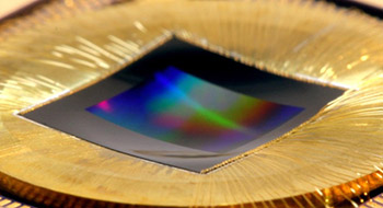
Infrared radiation image
Seeing into the Future of Infrared Detectors
Infrared radiation, the part of the electromagnetic spectrum invisible to the human eye, is a key enabling component in a myriad of technologies, spanning from communication to medicine to astronomy.
As infrared detectors and imagers continue to improve, they approach the theoretical limit of their performance, typically related to thermodynamics, or to the quantum nature of light.
In a paper titled, “Recent Advances in Infrared Imagers: Toward Thermodynamic and Quantum Limits of Photon Sensitivity,” published in March in the journal Reports on Progress in Physics, Professor Hooman Mohseni and PhD student Simone Bianconi present a perspective of the future of this technology. The paper shows simple yet powerful analytical models to evaluate these theoretical limits and guide novel device design toward improved performance.
One of the most powerful approaches, the authors argue, is to shrink the size of pixel detectors, taking advantage of nanoscale phenomena to improve the device sensitivity and bandwidth, while simultaneously increasing the resolution and lifting the constraints on the size and weight of the optics. The main challenge, the paper emphasizes, is how to effectively couple light to small devices, below the diffraction limit. The paper offers potential solutions.
Curved infrared imager
Finally, the paper discusses novel device concepts inspired by nature, such as a curved imager mimicking the retina, or smart read-out systems capable of processing and filtering images in real time in the same way a human brain would.
Seeing into the Future of Infrared Detectors
A new paper by Professor Hooman Mohseni and PhD student Simone Bianconi shows simple yet powerful analytical models to evaluate the theoretical limits of infrared technology and guide novel device design toward improved performance.
 www.mccormick.northwestern.edu
Main source
Recent advances in infrared imagers: toward thermodynamic and quantum limits of photon sensitivity
Academic's publication archive

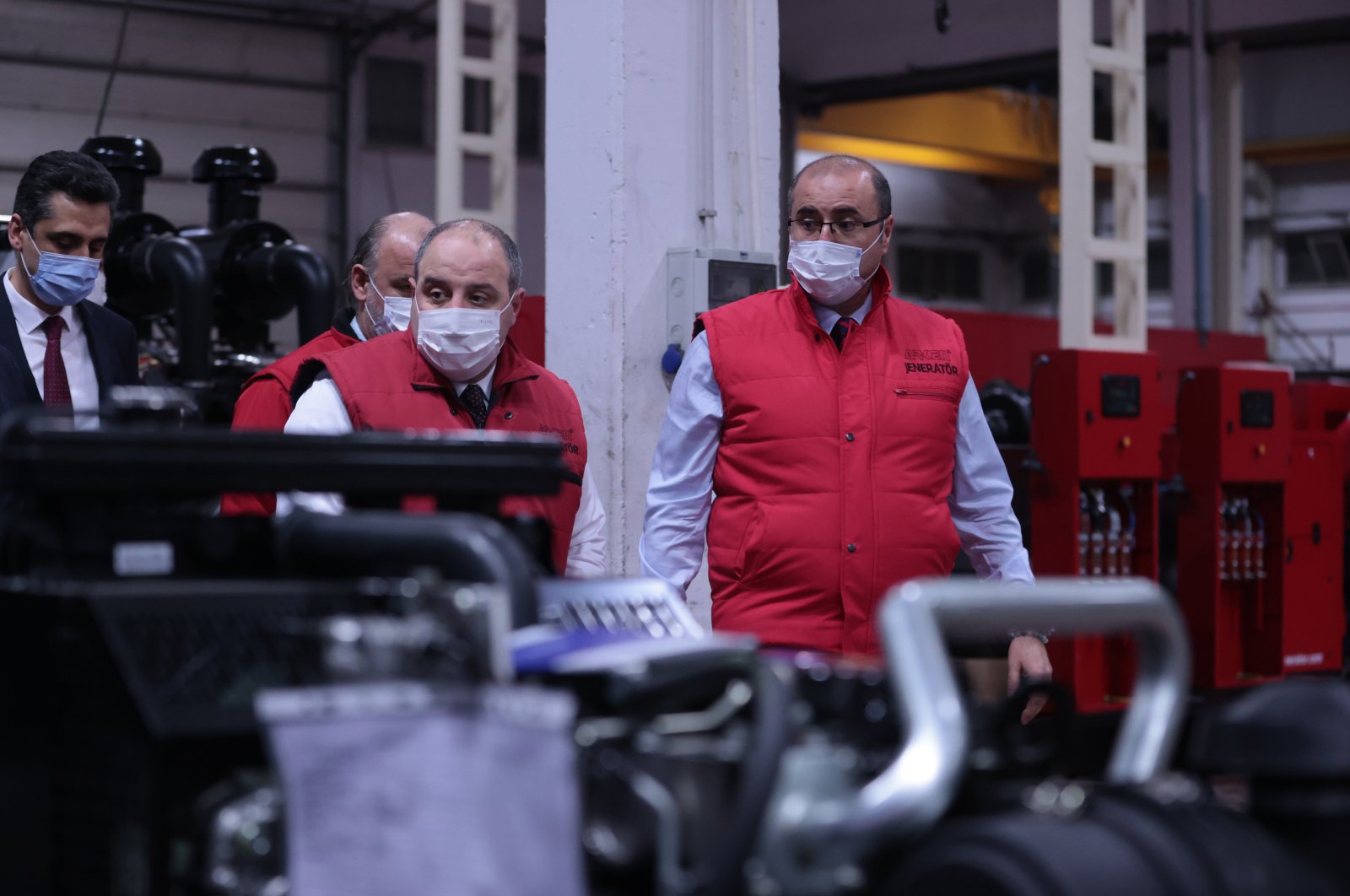
Turkish firm builds world's first fully biodiesel generator
A Turkish company has built a prototype for the world’s first generator that runs solely on biodiesel fuel, Industry and Technology Minister Mustafa...
E
ekemenirtu
Guest
In a paper titled, “Recent Advances in Infrared Imagers: Toward Thermodynamic and Quantum Limits of Photon Sensitivity,” published in March in the journal Reports on Progress in Physics, Professor Hooman Mohseni and PhD student Simone Bianconi present a perspective of the future of this technology. The paper shows simple yet powerful analytical models to evaluate these theoretical limits and guide novel device design toward improved performance.
There is no intention to derail the discussion towards politics. I find it somewhat ironic that an Iranian professor would be working to advance the state of the art in science and/or technology for what has been dubbed the "Great Satan" or the "global arrogance". Perhaps those descriptions are very apt and justifiable.
What is interesting is that out of close to 200 countries that the talented Iranian researchers could opt for, they choose the "Great Satan" or the "Global Arrogance" more often than any other country.
This is perplexing.
Nevertheless, I thank mod @Bogeyman for updating us on an important issue.
A good follow on to quoted discussion in this documentary (esp at ~ 22 minute mark, though entire thing is a good watch):
@MisterLike @anmdt @Vergennes @Constan @Paro @kaykay @T-123456 @Kartal1 @Sinan @xenon5434 @VCheng @Saiyan0321 et al. may also find interesting
next next frontier is going to be countries forming coalitions and start sectioning off the planets - Moon, Mars, Europa ...
Thats not far off to be honest.
Probably there will be informal cooperation and understanding.
Officially something like Antarctic treaty will be done, as is has set precedence right here on Earth (considering the vast mineral and energy resources of Antarctica).
Something will be worked out given multi-polar world and game theory issues (when things are too delineated and conflicts/tensions uneccesarily created).
Lot depends on what kind of technology we have unlocked at that point and what resources are even the relevant ones....it might not be anything like what we have now....so we aren't thinking in the relevant way to project (since we do that with what we have established as of this moment rather than what potentially could develop).
@MisterLike @anmdt @Vergennes @Constan @Paro @kaykay @T-123456 @Kartal1 @Sinan @xenon5434 @VCheng @Saiyan0321 et al. may also find interesting
Global Business Press | GBP
 gbp.com.sg
Rolls-Royce Starts Building World’s Largest Aero-engine
Rolls-Royce has officially started building the world’s largest aero-engine, UltraFan.
Work on the first module is underway at our dedicated DemoWorks facility in Derby, UK, and the demonstrator engine, which has a fan diameter of 140 inches, will be completed by the end of the year.
The engine is the basis for a potential new family of UltraFan engines able to power both narrowbody and widebody aircraft and deliver a 25% fuel efficiency improvement compared with the first generation of Trent engine.
Gas turbines is expected to continue to be the bedrock of long-haul aviation for many years, and UltraFan’s efficiency will help improve the economics of an industry transition to more sustainable fuels, which are likely to be more expensive in the short-term than traditional jet fuel. The first test run of the engine will be conducted on 100% Sustainable Aviation Fuel.
Rolls-Royce and a variety of funding agencies, including the Aerospace Technology Institute and Innovate UK (United Kingdom), LuFo (Germany) and Clean Sky Joint Undertaking (European Union) are involved in the project.
As engine build starts, other key parts are already coming together for delivery to Derby. Work is underway on UltraFan’s carbon titanium fan system in Bristol, UK, and its 50MW Power Gearbox, which is powerful enough to run 500 family cars, in Dahlewitz, Germany.
“This is an exciting moment for all of us at Rolls-Royce,” said Chris Cholerton, Rolls-Royce, President – Civil Aerospace. “Our first engine demonstrator, UF001, is now coming together and I’m really looking forward to seeing it built and ready for test. It is arriving at a time when the world is seeking ever more sustainable ways to travel in a post-COVID 19 world, and it makes me and all our team very proud to know we are part of the solution.
UltraFan is part of Rolls-Royce’s IntelligentEngine vision; each fan blade has a digital twin that stores real-life test data, allowing engineers to predict in-service performance. When on test at Rolls-Royce’s £90m Testbed 80 facility, data can be taken from more than 10,000 parameters, detecting the tiniest of vibrations at a rate of up to 200,000 samples per second.
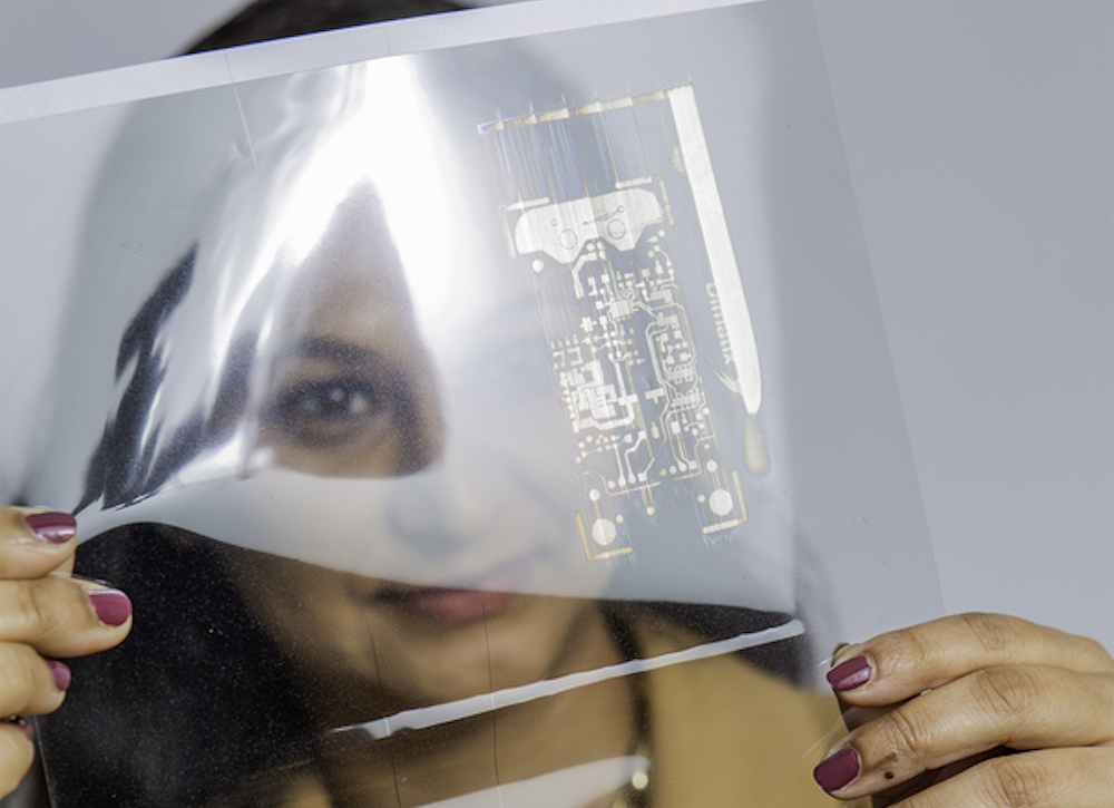
Toward a flexible future: A review on droplet-based techniques for fabricating printed electronics
When talking about additive manufacturing, we often imagine using these techniques to create large-scale 3D objects such as ceramic implants, turbine parts, or even homes. But by its nature, additive manufacturing excels at creating much less bulky devices as well, such as printed electronics.
“Printed electronics (PE) is an emerging technology under the umbrella of additive manufacturing that uses functional inks to print circuits and electrical components on various substrates,” researchers explain in a recent paper. “So far, PE has enabled fabrication of devices including but not limited to thin film solar cells, antennas, memories, transistors, displays, batteries, capacitors, and sensors.”
The researchers are led by Shweta Agarwala, assistant professor of electrical and computer engineering at Aarhus University (Denmark). She is joined by professor Preben Kidmose and Ph.D. student Hamed Abdolmaleki.
In an Aarhus press release, Abdolmaleki explains that compared to conventional lithography-based techniques for fabricating semiconductors, which use light to transfer a predefined pattern onto a rigid substrate, printed electronic techniques open “a plethora of new possibilities to print flexible electrical circuits directly onto a wide range of substrates such as plastics, papers, clothes, and quite literally any other planar and non-planar surfaces.”
Research on printed electronics is advancing quickly, so keeping abreast of the latest discoveries is challenging. “Through this paper, we have tried to fill the existing void in literature by discussing techniques, material inks, ink properties, post processing, substrates and application to provide a complete guide,” Agarwala says in the press release.
Below is a brief summary of the main findings from the 29-page review paper.
Types of printing processes
Printing processes can be broadly classified as “contact” and “noncontact.” In contact printing, ink is transferred directly from a patterned medium (such as an engraved roller or stencil) onto a substrate. In noncontact printing, ink droplets are ejected from a series of nozzles onto the intended surface.The authors focus this review on the latter category of noncontact printing, which consists mainly of three droplet-based printing techniques: inkjet, aerosol‐jet, and electrohydrodynamic‐jet printing.
Inkjet technology is the most widely used noncontact method for printing electronics.
In this technique, ink droplets are ejected onto a substrate via either continuous inkjet or drop‐on‐demand ejection modes. In the former method, a continuous column of ink ejects from a nozzle and spontaneously splits into droplets due to an acoustic wave generated by a piezoelectric ceramic. In the latter method, ink droplets are ejected in a controlled manner by passing trigger signals through actuators (either thermal or piezoelectric) located within the printhead.
Compared to the other noncontact printing techniques, inkjet printers have fewer operating parameters and so can reach optimal printing conditions more easily and in less time.
Aerosol jet technology is relatively new compared to inkjet technology, yet researchers have already successfully used this technique to fabricate transistors, lithium-ion batteries, and solar cells, among other devices.
This technique involves formation and deposition of an aerosol on a substrate. “Aerosol” is defined as a suspension of liquid or solid particles in a gas carrier. While techniques to produce and deposit aerosols have been known since the mid‐20th century, only recently has the technology to control aerosol jet deposition by digital signals been developed.
Compared to the other noncontact printing techniques, aerosol jet printers have enhanced capabilities for printing complex designs on 3D substrates (rather than just planar substrates) and have relaxed requirements for ink rheology and fluid mechanic properties.
Electrohydrodynamic jet printing was patented in 1998 by Choi and Smith, but it wasn’t until 2007 that researchers at the University of Illinois at Urbana-Champaign significantly enhanced the resolution for printed electronics.
This technique uses an electric field to create fluid flow from the nozzle to the substrate. Flow rate and electrical field are two important parameters that determine the jetting behavior of inks. When these parameter values are low, droplets are ejected from the nozzle by gravitational forces in a “dripping” mode. As the values of these parameters increase, droplets are ejected in a “pulsating” mode and, at even higher values, a “cone-jet” mode.
Compared to the other noncontact printing techniques, electrohydrodynamic jet printers cater particularly to printing resolutions smaller than 100 nm, which is promising for printing cells and tissues for biotechnology and biomedical applications.
Types of functional inks
To date, researchers have explored several kinds of organic and inorganic materials for printed electronics. While organic materials show better flexibility and processibility, inorganic materials often possess better electrical properties.A functional ink typically has four constituents:
- Solvent—The solvent dissolves or disperses the other three constituents and tunes the ink’s final viscosity.
- Functional material—The functional material endows the ink with electrical properties.
- Polymer binder—The polymer binder minimizes intermolecular interactions between nanoparticles, thus increasing the ink’s stability and shelf life.
- Additives—The additives enhance stability and performance. The most widely used additives are dispersing agents (surfactants), rheology modifiers, defoamers, plasticizers, and biocides.
For metal inks, silver is the most widely used functional material due to its outstanding electrical conductivity and high chemical resistance. Gold, though expensive, is used as well due to its high functionality and superior chemical stability, which makes it a preferred choice for applications involving corrosive and extreme environments. Copper is considered a low-cost alternative to silver and gold, but it can undergo rapid oxidation when exposed to ambient oxygen and thus is difficult to handle.
For carbon-based inks, graphene and carbon nanotubes are widely used. Graphene inks are prepared using four main approaches: oxidative exfoliation, sonication‐induced exfoliation, shear exfoliation, and electrochemical exfoliation. Preparing carbon nanotube-based inks is difficult because of the material’s poor dispersion in water and organic solvents, but researchers have devised several physical and chemical strategies for overcoming this challenge, such as using different dispersants or surface modification techniques.
Polymer inks are of high interest due to excellent mechanical compliance and easy processability via solution‐based methods. There are two main classes of functional polymers: conjugated polymers and electroactive polymers. In general, conjugated polymers show poor device performance and low charge carrier mobility due to their semicrystalline nature. In contrast, electroactive polymers are highly sought after due to their ability to change size and shape in response to an electrical field, which is a useful characteristic for fabricating sensors and actuators.
Ceramic inks can show interesting electrical properties, such as superconductivity, semiconductivity, piezoelectricity, and magnetic features. For ceramic inks to yield a uniform pattern when printed, they should fulfill three main requirements: 1) adequate particle size and stability of the suspension, 2) proper fluid mechanics, and 3) proper drying behavior.
Limiting factors and challenges
After reviewing post-processing methods and types of substrates, which you can read more about in the paper, the authors conclude by detailing some areas in which research and innovation are needed to push this emerging technology toward commercialization. For example,- Printability—Printability is the ability of a final product to follow the initial computer designed pattern. However, most of the software used for printed electronics have constraints on curved edges or multilayer designs, which restricts the design possibilities. In addition, due to fluid mechanic requirements, the viscosity and solid content of inks cannot exceed a certain value, meaning many printing passes may be required to achieve a thicker printed pattern.
- Device fabrication—An encapsulation layer is typically used to protect printed electronics, which are prone to damage due to their thin and flexible nature. However, challenges with choosing an encapsulation layer include elastic constant mismatch, thermal expansion mismatch, and stress concentration from the layer to the printed circuit.

Toward a flexible future: A review on droplet-based techniques for fabricating printed electronics - The American Ceramic Society
Researchers from Aarhus University reviewed processing techniques, ink materials, substrates, and sintering methods for printed electronics.
 ceramics.org
Main article

(PDF) Droplet‐Based Techniques for Printing of Functional Inks for Flexible Physical Sensors
PDF | Printed electronics (PE) is an emerging technology that uses functional inks to print electrical components and circuits on variety of substrates.... | Find, read and cite all the research you need on ResearchGate
 www.researchgate.net
IBM 2nm chip breakthrough claims more power with less energy
The process used to make computer chips is measured in nanometres (nm) - with a lower number usually signifying a leap forward.
IBM claims its test chip can improve performance by 45% over current 7nm commercially available products.
It is also more energy efficient - using 75% less energy to match current performance, IBM said.
It claims the tech could "quadruple" mobile phone battery life, and phones might only need to be charged every four days.
The computer chip industry used to use nanometres - one billionth of a metre - to measure the physical size of transistors. Today, a lower "nm" number is widely seen as a marketing term to describe new generations of the technology, leading to better performance and lower power.
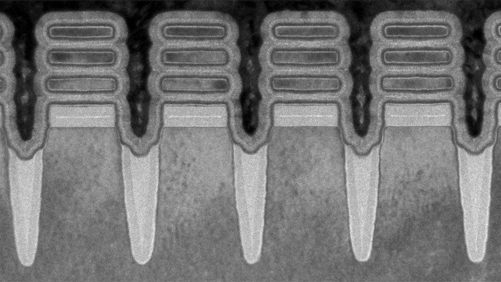
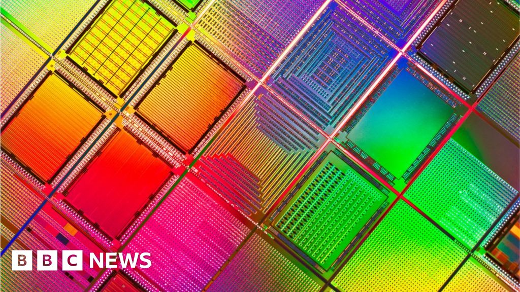
Transistors on the IBM "nanosheet" it uses for the new tech
IBM says its 2nm process can cram 50 billion transistors into "a chip the size of a fingernail" - up from 30 billion when it announced its 5nm breakthrough in 2017.
The end result should be another performance bump for computers in the coming years.
'A breakthrough'
Current high-end desktop chips based on the 7nm process, such as AMD's Ryzen processors, did not become widely available until 2019 - four years after IBM announced it had cracked the 7nm process.But mainstream commercial chip-makers such as Intel and TSMC - which makes AMD processors - have already said they plan to build ultra-low nm chip plants in the next several years.
"This can be considered as a breakthrough," said Peter Rudden, research director at market intelligence firm IDC.
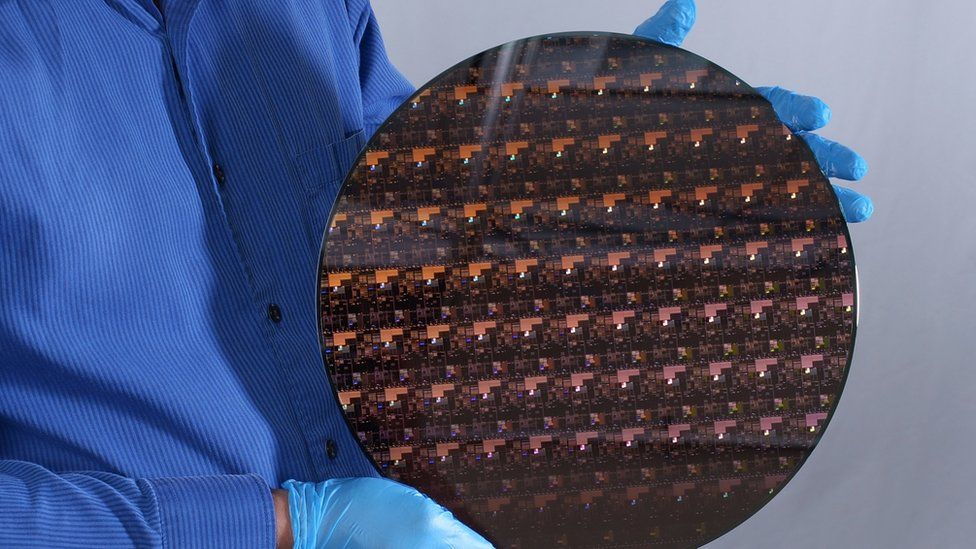
The chip wafer for the 2nm chip, held by an IBM employee
"We have seen semiconductor manufacturers moving from 14nm to 10nm to 7nm, with 7nm being a real challenge for some," he explained.
He said IBM's new process could be used for AI uses that today need a second piece of tech - such as a powerful graphics card- to handle some tasks. The increased power efficiency could be useful in personal devices, while increased performance would benefit huge datacentres, he added.
"This also sends a message to the IT industry that IBM continues to be a hardware research powerhouse."
Chip wars
IBM said the test chip for its 2nm process was built at its Albany research lab in the United States.The news comes amid an international shortage of computer chips and a bid to shake up chip manufacturing to rely less on major foundries in China and Taiwan.
Car manufacturers have been forced to suspend production due to the lack of computer parts; smartphone makers have warned product releases could be affected; and high-end computer components such as graphics cards are difficult to find and selling for high prices.
On Thursday, Nintendo joined the chorus of concerned companies, saying the chip shortage was affecting production of its hugely popular Nintendo Switch console.
The worldwide shortage led US President Joe Biden to convene a special industry summit on the shortage. In the UK, the government has intervened in the acquisition of chip designer Arm by tech giant Nvidia.
And Intel's chief executive has announced a $20bn (£14.6bn) investment in two new plants in the US, telling the BBC that having 80% of the world chip supply in Asia is not a good idea.
IBM 2nm chip breakthrough claims more power with less energy
Next-gen processor tech gives more performance with less energy use, IBM claims.
 www.bbc.com
Looks like fur.
A very warming one.
Looks like fur.
A very warming one.
Magnetic field lines and plasma!
Sent all replies from "Science and Engineering" thread that was in hobby section to this thread to make a mega thread (effectively merging them).
Should be even more interesting read + interaction now hopefully.
Should be even more interesting read + interaction now hopefully.

NASA awards Turkish technology firm - Latest News
NASA awarded Turkish nanotechnology firm Nanosilver, which conducts research and development activities in Turkey's Teknopark Istanbul, with a nanosized silver project.

According to article whatsapp is suing India for demanding violation of privacy by tracking messages.

SpaceX CRS-22 Mission Overview
SpaceX’s 22nd contracted cargo resupply mission with NASA to the International Space Station will deliver more than 7,300 pounds of science, research, crew supplies, and vehicle hardware, including new solar arrays, to the orbital laboratory and its crew. This is the second mission under SpaceX’s Commercial Resupply Services-2 contract with NASA. Launch is targeted for Thursday, June 3, at 1:29 p.m. EDT. Launch activities will air live on NASA Television, the NASA app, and the agency’s website.Live

Research Highlights
Hundreds of experiments are being conducted on the International Space Station in the areas of biology and biotechnology, physical sciences, and Earth and space science. This research helps us better understand how to prepare for future long-duration missions to the Moon and Mars, supports a growing space economy, and leads to developments that improve life on Earth. The SpaceX cargo spacecraft will deliver dozens of investigations to the International Space Station, including:- Research that could help develop cotton varieties that require less water and pesticides
- An experiment looking at tardigrade survival in space, which could advance understanding of the stress factors affecting humans in microgravity
- A portable ultrasound device
- A new way of providing tactile and visual feedback to astronauts during robotic operations
- A look at interactions between beneficial microbes and their animal hosts
These and other cutting-edge investigations join the hundreds of ongoing experiments aboard the orbiting laboratory. To learn more, check out our research highlights story.
Cargo Highlights
SpaceX’s Falcon 9 rocket will send the company’s Dragon spacecraft, filled with more than 7,300 pounds of research, crew supplies and hardware to the space station to support expeditions 65 and 66.*Cargo weights subject to change

Hardware
Launch- ISS Roll-Out Solar Arrays (IROSA) – Solar arrays launching for installation during the summer 2021 spacewalks to upgrade power capabilities on-orbit
- Catalytic Reactor - Legacy unit launching to provide critical sparing support for the water production capability for the environmental control and life support system (ECLSS)
- Commercial Crew Vehicle Emergency Breathing Air Assembly (CEBAA) Regulator Manifold Assembly (RMA) - Completing the first setup for emergency air supply capability, this integrated system supports as many as five crew members for up to one hour during an ISS emergency ammonia leak
- Zarya control module Kurs electronics unit - Critical hardware for cosmonaut remote-control docking of Russian spacecraft is launching to support planned maintenance activity during 2021
- Potable Water Dispense (PWD) Filter - Major filter assembly used to remove iodine from water consumed by the crew during nominal operations
- Commercial off-the-shelf (COTS) Air Tanks - Critical disposable air tanks to support gas resupply for routine cabin repress activities on-orbit
- Iceberg - Critical cold stowage capability to support expanded payload operations
Return:
- Catalytic Reactor Developmental Test Objective (DTO) - Developmental environmental control and life support system (ECLSS) unit returning for testing, teardown, and evaluation (TT&E) to determine the cause of failure and subsequent re-flight
- Urine Processing Assembly (UPA) Distillation Assembly - Critical ECLSS orbital replacement unit used for urine distillation, processing, and future use returning for TT&E and refurbishment to support future spares demand
- Sabatier Main Controller - Major Sabatier system hardware used in conjunction with the Oxygen Generation System (OGS) for water production needs on-orbit
- Rodent Research Habitats (AEM-X) - Habitats used during Rodent Research missions returning for refurbishment to support future missions in early 2022
- Nitrogen/Oxygen Recharge System (NORS) Recharge Tank Assembly (RTA) - Empty gas tanks returning for reuse to support high-pressure gas operations and activities on-orbit
Food for the Crew
Many resupply missions include provisions for the residents of the space station, and SpaceX CRS-22 is no exception. Crew members can expect to unpack the following foods during this mission:Fresh food
- Apples (Gala)
- Oranges (Navel)
- Tomatoes (Cherry Style)
- Onion
- Lemons
- Peppers (mini)
- Avocados
15 Standard Menu Food Containers
30 Crew Specific Menu and Coffee Tea Preference Containers
10 Food Physiology Containers
Watch & Engage
Live coverage of the launch from Pad 39A from NASA’s Kennedy Space Center will air on NASA Television, the NASA app, and the agency’s website on June 3 at 1 p.m. ET with liftoff at 1:29 p.m. ET. The prelaunch news conference will be live at 1:30 p.m. ET on Wednesday, June 2.Arrival & Departure
The Dragon spacecraft will arrive at the space station and autonomously dock to the space-facing port of the Harmony module on the International Space Station at approximately 5 a.m June 5. Coverage of the rendezvous and docking will begin at 3:30 a.m. NASA astronauts Shane Kimbrough and Megan McArthur will monitor the arrival of the spacecraft, which will stay aboard the orbiting laboratory for about a month before splashing down and returning critical science and hardware to teams on Earth.
trishna_amrta
Experienced member

Unfortunately, in tropical region such as South East Asia, solar photovoltaic power is neither efficient let alone economical no matter the scale. Which is the main reason I avoid using it and sticking to burning dino-juiceEveryone owes it to themselves (if they haven't already) knowing the basics of semiconductor solar technology, given it is going to be a huge increasing part of electricity generation profile in the years to come.
This video does a very good job in laying out the basics:
For those that would like a bit more expansion on where the improvement in efficiency is broadly headed....it is by use of a larger profile of semiconductor materials (that have different band gaps to silicon and thus able to use more of the incident sunlight emission spectrum when you multi-layer and multi-junction by stacking them up etc...given lot of these materials are not constrained by silicon's "indirect bandgap" which wastes energy by lattice vibration)
A good summary of this can be found here for those interested:
There are of course engineering, design and cost challenges of this approach (you will notice the page is from 2002) and this forms the ongoing research and development of this technology currently.
Some of the recent news on it (multijunction):

Scientists Propose Technology That Could Reduce the Cost of High-Efficiency Solar Cells - Mercom India
The scientists of St. Petersburg University in Russia have tested a new technology for the fabrication of high-efficiency solar cells based on A3B5 semiconductors integrated on a silicon substrate....mercomindia.com