India Indian Economy + Infra Archive

Afif

Experienced member
Moderator
Bangladesh Correspondent
DefenceHub Diplomat
Bangladesh Moderator
Messages
4,051
Reactions
64 7,390
Nation of residence
Bangladesh
Nation of origin
Bangladesh
Is this actually a good thing though? Considering the size of economy and GDP per capita.
Same is true for Pak and BD.
Personally i think, we need better family planning. Then again, some people would argue, given majority of this population is young it is actually a good work force with a lot of potential.
 

Nilgiri

Experienced member
Moderator
Aviation Specialist
Messages
9,327
Reactions
96 18,910
Nation of residence
Canada
Nation of origin
India
Is this actually a good thing though? Considering the size of economy and GDP per capita.
Same is true for Pak and BD.
Personally i think, we need better family planning. Then again, some people would argue, given majority of this population is young it is actually a good work force with a lot of potential.

Demographically, India+Bangladesh will have a better time longer term than China, given what China did way too drastically and now has to handle its inverted population pyramid for this century (the problems are just commencing now on that).

India and BD should try keep their TFR around 2 as far as possible and not let it get too low....so there is not too rapidly aging (and fiscal support pressure from worker dependency ratio for elderly support etc).

Problems concerning this are already affecting parts of South India for example where TFR is now 1.5 or even lower....though there is internal migration from North India picking up somewhat to address it.

Then keep investing in human resource development (this is the key thing, that separates South and West India from North India for example in the bulk population medians).

BD seems to have picked up on lot of this and will continue in its way as well....the route is proven and clear.

Pakistan is very different problem in other direction (compared to IND and BD).

Its TFR is still very high (higher than 3), not coming down quick enough...and its establishment have mismanaged things awfully and are stuck in real grave predicament now.
 

Nilgiri

Experienced member
Moderator
Aviation Specialist
Messages
9,327
Reactions
96 18,910
Nation of residence
Canada
Nation of origin
India

Inside Vedanta's gigantic semiconductor ambitions​

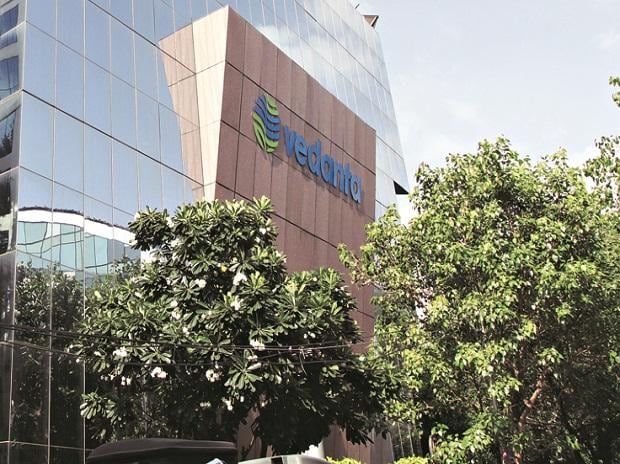
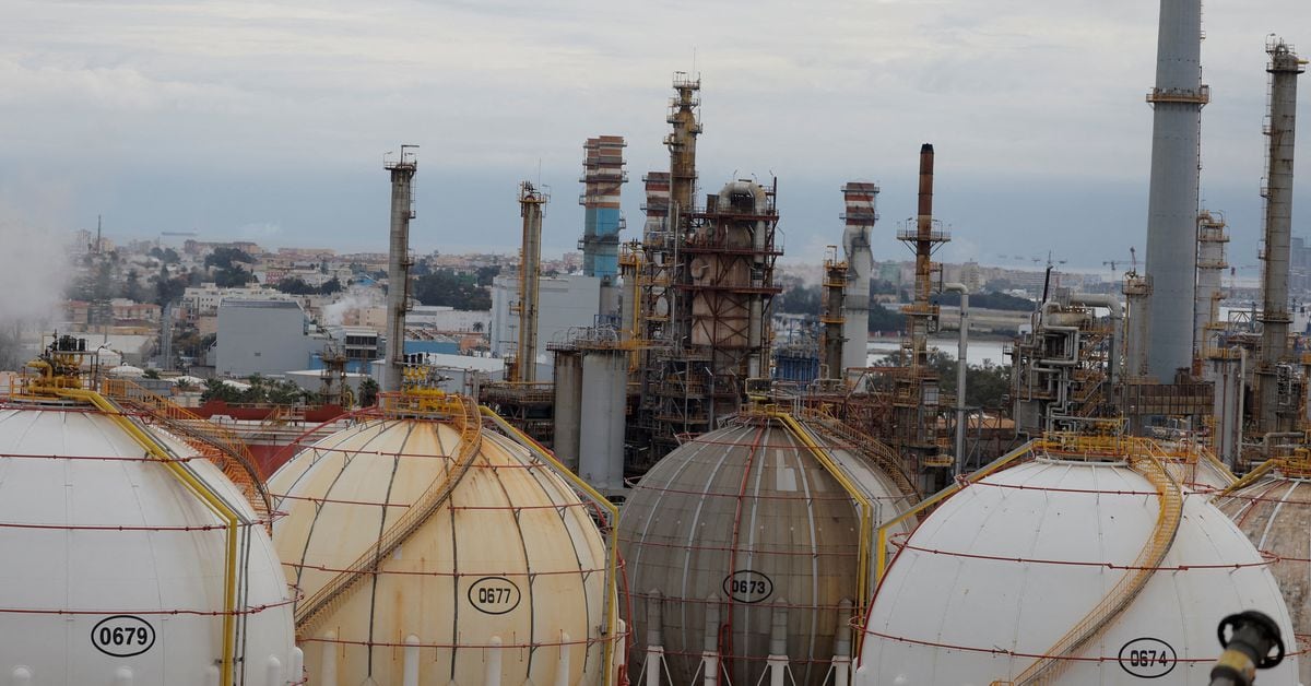
The company is betting big on a novel ecosystem to develop around India's semiconductor and glass manufacturing industries. The entire project is estimated to cost Rs1.54 lakh crore and will involve a bunch of risk takers and entrepreneurs

BY MANU BALACHANDRAN, Forbes India Staff
14 min read
PUBLISHED: May 11, 2023 02:08:40 PM IST
UPDATED: May 11, 2023 04:55:38 PM IST


For Akarsh Hebbar, the watershed moment came sometime in late 2017.

The son-in-law of metal and mining magnate Anil Agarwal, Hebbar had been carefully avoiding the lure of joining the family business since his marriage to Priya Agarwal in 2013. Instead, the 35-year-old went on to study at the London School of Business, before joining global consultancy McKinsey as an associate after a brief internship at Google.

McKinsey became his ‘target’ primarily because it had a business technology consultancy arm, which would allow Hebbar—a confessed aficionado of technology—to work with the world’s top technology companies. “I was traveling all over the world doing that,” says Hebbar, who had previously worked with Oracle in India, Japan and Jordan.

Then, the inevitable happened. “One day, my father-in-law, says, Yeh kya professional job kar raha hai? [Why are you doing this professional job?]. Let him see our business.” To begin with, Agarwal, the chairman of Vedanta Resources, with interests spanning mining, oil and gas, and electric utility among others, tried coaxing his son-in-law into the world of mines, the mainstay of the family fortune.

“I was very bored,” Hebbar says. “What am I going to do with the mines?”

Thankfully for Hebbar, Agarwal’s ploy came up at a time when the family had set its eyes on AvanStrate Inc, a financially struggling Japanese manufacturer of LCD glass substrates. The acquisition was expected to give a fillip to Vedanta’s plans of setting up India’s first plant to make flat panel displays for televisions (TV) through its arm, Twin Star Display Technologies. Coincidentally, the billionaire had engaged McKinsey for due diligence on the asset.

“I looked at it as part of McKinsey and found it amazingly interesting,” Hebbar says. “I thought it was a pearl in the ocean and I said you should definitely go for it.” That firm tone of approval from his son-in-law, who had by then become rather obsessed with the stunning Japanese technology to manufacture thin display glasses, certainly was music to the ears of 69-year-old Agarwal. He then asked Hebbar to lead the distressed AvanStrate, which Vedanta acquired for $158 million in December 2017.


Also read: India woos semiconductor makers in quest to become key player

“The future in India is only for two or three things,” Agarwal tells Forbes India over a video call from London. “Seventy percent of our import are between natural resource and electronics. For electronics, the basic raw materials are chips and glass. So, I thought that if I can hold on to AvanStrate, I can build on that foundation.”

Today, it’s that decision that has given Vedanta enough ammunition to try and build India’s first semiconductor and glass display manufacturing facility. It has set up two subsidiaries, Vedanta Foxconn Semiconductors Limited (VFSL), which will set up a fab foundry to manufacture 28 nanometre (nm) and 40 nm wafers (slices of semiconductor material used to make integrated circuits), and Vedanta Displays Limited (VDL) that will make glass panels for applications such as TV, IT, automobiles and smartphones.

The entire project is estimated to cost Rs1.54 lakh crore, with the central government providing a 50 percent subsidy to both projects, as part of its $10 billion (Rs76,000 crore) Indian Semiconductor Mission package to promote semiconductor manufacturing in India.


Inside Vedanta's gigantic semiconductor ambitions


Vedanta has already tied up with Taiwanese technology company Hon Hai Precision Industry, commonly known as Foxconn, for its semiconductor business. The joint venture has also brought on David Reed as the CEO of Vedanta Foxconn Semiconductors Limited. Reed, an industry veteran with over three decades of experience, previously worked with Dutch chip company, NXP Semiconductors, and GlobalFoundries.

“Semiconductor chips are the brains of every device,” explains Hebbar, who is now the global managing director of Vedanta’s semiconductor and display business. “We're also looking at the display ecosystem, which are the eyes of everything. Together they make up 60 percent of any electronic device. With our project, we are becoming the nucleus for electronic manufacturing.”


What’s Vedanta’s plan?​

Minister of Electronics and Information Technology Ashwini Vaishnaw had said last August that a decision on semiconductor approvals often takes between 14 and 16 months. By that estimate, the Indian government, which accepted applications in January 2022, is likely to give project approvals in the next few months.

Therefore, Vedanta reckons its applications are in their last mile run, even as it has almost firmed up land for its project in Gujarat. “We are going ahead,” Agarwal says. “Land has been allotted and the partnership with Foxconn has been tied up.”

On its part, Vedanta says it has met all the criteria laid out by the government. Vedanta holds a 63 percent stake in the semiconductor project, while Foxconn holds the remaining. The partnership, a first-of-its-kind in India, was stitched on mutual trust, and a strong belief by Foxconn that Vedanta is swift with their act, Agarwal says. “There cannot be two drivers on a car,” Agarwal says. “Young Liu, (Foxconn’s chairman) suggested that, because you are the son of the soil, you drive the car, and we'll sit by the side. They will take full responsibility on the technology side.”

“We realised very early on that what Vedanta has, Foxconn doesn't, and what Foxconn has, Vedanta doesn't,” Hebbar explains. “We have different revenues and different business streams. The forte that we have in manufacturing and business in India and the forte that they have in the technology ecosystem are complementary to each other.” Foxconn will be fully responsible for the operations and sales, and also the entire technology of the project.

Besides, the partnership is looking to acquire new licenses as quickly as it can as semiconductor technology undergoes a significant shift. “Semiconductor is such a business that we're acquiring production licenses every single day,” Hebbar says.


Also read: Why isn't Apple worried about Taiwanese chips?

Foxconn has roped in a technology partner with a production-grade licence and expertise in manufacturing, as per government requirements. Vedanta, however, doesn’t want to divulge details about this company, although there were rumours of talks with STMicroelectronics. The company has also roped in Terry Daly, an IBM veteran and former senior vice president at GlobalFoundries, as an advisor for its semiconductor business.

“We have a very strong partner whose name we will reveal later, but they are a high volume, industrial automotive grade, 40 nm technology player,” Hebbar says. “When you're talking about automotive grade and industrial grade, you are surpassing every other grade, because of the safety nature of automotive.”

VFSL’s integrated semiconductor fab foundry will have the capacity to manufacture 40,000 wafers per month to cater to mobiles, consumer electronics, automotives, and network equipment. “We have got the technology partner, we have got the technology agreements, the definitive agreements, and submitted them to the government,” says Hebbar. “As our application gets processed, it will go through the most stringent process, to make sure we are not only the first but also the example for 10 more companies to come.”

“I liken this (project) to a Wernher von Braun moment [father of space travel] for India,” says Reed, who has recently made the shift to India. “This is an opportunity to bring the world's best talent from around the world, and everybody's interested in the world's first Indian production wafer plant.”


Inside Vedanta's gigantic semiconductor ambitions


David W. Reed, CEO Vedanta Semiconductor. Image: Amit Verma


Also read: Will India's PLI Scheme help it transform into a semiconductors powerhouse?

Meanwhile, in its glass display business, Vedanta has tied up with Taiwan-based InnoLux Corporation as its partner. The Taiwanese company was already AvanStrate’s client, which made the partnership an easy one to stitch. VDL will focus on Gen 8.6 A-Si IPS fabs, including glass, panel, and module with a per-month capacity of 60,000 sheets and 10 nm modules to cater to TV, IT, automobiles and smartphones.

“India has 25 percent of the world's population, which means there is captive demand,” Hebbar says. “Our import bill for electronics was $53 billion, about two-and-a-half years ago, but now it's close to $100 billion and that's going to become $400 billion by 2026-27. We are making this in India because we have the required assets. India is going to be the fifth country in the world that's going to have this ecosystem.”


The big semiconductor focus​

Despite Vedanta’s glass display ambitions and expertise, all eyes are on its semiconductor business, primarily because of the ongoing shortage of semiconductor chips. “Between 2016 and 2020, the consumption of semiconductors doubled in India,” Hebbar says. “It was about $12 billion, which became $20-25 billion, and that is going to double again in the next few years and by 2030 will be $80-100 billion.”

The global semiconductor shortage was further aggravated by the Covid-19 pandemic, largely due to supply chain disruptions, with companies in Taiwan and South Korea shutting down, and demand for new devices soaring. This made global companies look at a diversified supply chain to combat the crisis.


Also read: How the global chip shortage is creating new power players

Semiconductors are critical components in consumer electronics. In vehicles, for instance, they are the mainstay of control and entertainment systems, and domestic automakers have faced severe production delays in the past few years. “At the height of the chip shortage, global auto production slumped 26 percent during the first nine months of 2021,” says a JP Morgan report.

Vedanta has now signed Memorandums of Understanding (MoU) with companies in Japan and South Korea, and reckons that an $80 billion ecosystem across semiconductors and display units can be built once Vedanta starts operations. What gives the company confidence about its plan is also its target of manufacturing 40 nm chips, which it believes will eventually help it make 28 nm chips, since the process is similar; 40 nm and 28 nm chips contribute to over 66 percent of the global demand for chips and are used in ICT devices and electric vehicles (EV), among others.


Inside Vedanta's gigantic semiconductor ambitions


“Eighty to 85 percent of the 40 nm process is used in the 28 nm process,” Hebbar says. “Foxconn is an expert in this. They are not just the technology transfer company or assembly and test company. They're an industry transfer company. They will also bring the entire industry with them. They've done that in China, they're going to do it in India.”

Then there is the massive captive demand that the joint venture is looking to tap into. India, according to Hebbar, does not require chips lower than 22 nm, such as those used in high-end phones such as iPhones. “I think we are making about 250 million smartphones, about 30 million TVs, and another 25 to 30 million notebooks. These all are not the highest-grade technologies,” he says. “We are making sure that we have a tried-and-tested technology and the market for it.”


Also read: Diversification away from Taiwan chipmakers is necessary

“Electronic imports worth $300 billion are next only to oil,” says Tarun Pathak, research director with Counterpoint Technology Market Research. “Vedanta can tap into that opportunity especially since government policies have become attractive. What they need to do is pitch their battle well and identify the focus areas. For now, they are rightly focusing on the older nodes which constitute 66 percent of the semiconductor demand. That was also where the shortage had happened. Now as companies want to de-risk from their focus on one country, India can offer a cost-effective alternative.” Counterpoint reckons that India’s semiconductor component market will see its cumulative revenues climb to $300 billion during the 2021-2026 period.

Alongside, Vedanta’s focus on display panels will allow manufacturers, especially new ones, to step forward and build their TVs, notebooks or mobile phones within the country, giving a big fillip to medium- and small-scale enterprises. “We are going to go through the same phase that China went through,” Hebbar says. “We will be able to build our own Oppo and Vivo. This is the kind of movement that we are going to bring about.”

But fuelling Vedanta’s grand ambitions won’t be cheap by any means. The project, which costs Rs1.54 lakh crore, will be partially funded by the government through its subsidy. State governments are also expected to dole out another 20 percent through various programmes, which significantly reduces the capital cost. Vedanta had been recently hit hard by its ballooning debt concerns, which had affected its liquidity, although the company has managed to pare it down by almost a billion dollars.

“Today, across the world, $3 trillion fund is available and not even 20 precent has been deployed for infrastructure or for semiconductors,” Agarwal says. “We will put 30 percent equity which we are comfortable with, and there will be a queue of people for the rest, because these kind of projects are not there in the world. There is enough water in the well for these kind of projects.”

“One of Vedanta's strengths is that we've raised $35 billion in the past,” Hebbar says. “And this is business as usual for us. All the banks know what our credibility is. We've never defaulted. We know how to make this project strategic business-wise. We want to be the first foundry, but we don't want to be the only foundry. India can develop about 20 to 30 foundries for its captive demand before it even thinks about exporting.”


Also read: How to lay the solid foundation for semiconductor fabrication in India

Besides, success in the semiconductor manufacturing business is also likely to help the company diversify into the outsourced semiconductor assembly and test (Osat) arena. Osats are companies that provide packaging and testing for silicon devices manufactured by foundries before their shipment to the market. “So, we are developing more downstream methodology,” Hebbar says,


Where does Vedanta go from here?​

For now, if everything goes according to plan, Vedanta foresees revenues from its semiconductor business starting in 2027. The company intends to start commercial production with 5,000 units of its 40 nm wafers, before going on to 15,000 units, and finally getting into 28 nm wafers. “From displays, revenues could come even earlier in 2025 end or 2026,” Hebbar says.

The company is working simultaneously on setting up its facility and hiring people, including expats with the right technical know-how. While it has identified Dholera in Gujarat as its primary location, it is also assessing other locations to make the project cost-effective. “Gujarat has very kindly offered to make the entire setup at Dholera conducive for our semiconductors,” Hebbar says. “But before we sign the final agreement with Gujarat, we'll have to have negotiations on land requirements and costs.”

In the glass display business, Vedanta claims to have tried-and-tested Gen 8 technology, and LCD technology for India, which is relevant for the next 10 to 15 years. Already, Hebbar says, AvanStrate is only one of four companies with the base glass-making capacity in the world, and its partner InnoLux makes automotive displays for the likes of Tesla.


Also read: The tech cold war's 'most complicated machine' that's out of China's reach

All that means Vedanta is now betting big on a novel ecosystem to develop around India’s semiconductor and glass manufacturing industries, with what Hebbar believes will be “bunch of risk takers and entrepreneurs who will come in” to build new products. “It is being created bigger than Silicon Valley,” Agarwal says. “It is the heart, and from that, it will pump into so many areas.”

Then there is also the potential that the sunrise sector offers in creating jobs. Already, Reed says there is significant interest from top talents across countries such as Japan, South Korea, Taiwan, Singapore, Malaysia, Europe, the US, Canada, and Mexico, who are keen to join the plan to build India’s first semiconductor foundry.

“We are looking at about 80,000 to 100,000 jobs being generated,” Hebbar says. “And this is just related to semiconductors and glass. When you're looking at MSMEs, you're looking at a higher number.” That’s because Vedanta expects India to have over 1,000 MSMEs who could be direct beneficiaries of semiconductor and display glass manufacturing, in addition to giving a boost to local technology transfer.

“This is not a five-year project,” Hebbar says. “This is not a 10-year project. It's a 20-year stabilisation of the entire semiconductor industry in India and this is the start of it.”

“What’s different this time, unlike in the past, is that the government appears to be more committed,” says Yugal Joshi, partner at Texas-based research firm Everest Group. “Today, while there is a growing sensitivity towards being self-reliant in the semiconductor space across Europe or the US, it may not be 100 percent possible. The industry is also cyclical with constraints and oversupply across various categories. India, meanwhile, should offer Vedanta with a captive market.”

The new opportunity also allows Vedanta to position itself strongly as a global technology company. “Vedanta is very focussed on making sure that we have a starting point, which is making 60 percent of the electronics,” Hebbar says. “But we can go downstream and start making phones or TVs. We make nickel, which means we have the raw material for EV batteries. We can acquire lithium when it comes. We're doing our evaluation to go into other businesses. This will be a new age business vertical.”

So, is Vedanta looking to capitalise on the first-mover advantage once its approvals come through? “We are not here to occupy the whole pie,” Hebbar adds. “There's enough pie for people to share. It will be a miss if India doesn’t take an opportunity like this and immediately capitalises on it.”
 

Nilgiri

Experienced member
Moderator
Aviation Specialist
Messages
9,327
Reactions
96 18,910
Nation of residence
Canada
Nation of origin
India

The centre is ready to approve the plans of the Vedanta-Foxconn joint venture to make semiconductor chips, a report in The Economic Times (ET) said. Senior government officials told the newspaper that this would be done under the aegis of the $10-billion India Semiconductor Mission (ISM).

With this plan, the government plans to establish India as a global hub for semiconductor manufacturing. The official was quoted in the report as saying, "Their plan is for fabrication of 40 nm (nanometre) chips — there are some conditions they need to fulfil. We are going to approve it."


To this end, Vedanta Foxconn Semiconductors Limited (VFSL) has signed agreements with two companies, GlobalFoundries and STMicroelectronics, to facilitate technology transfer. The report said the details of these two companies have been submitted to the Ministry of Electronics and Information Technology (MeitY).

Additionally, the government has directed VFSL to submit details of the "binding technology transfer agreement" with either of the two companies, the official aware of the developments said.


IT Ministry is the nodal ministry to oversee ISM. The ministry has suggested that GlobalFoundries and STMicro acquire a stake in VFSL. The two companies have responded positively to the suggestion, and their proposal is awaited.
VFSL is a joint venture between India's Vedanta Group and Taiwan's Hon Hai Precision Industry (Foxconn). The two have 63 and 37 per cent stake in the company, respectively.

The company is initially looking to invest Rs 66,000 crore (8 billion USD) to set up a semiconductor manufacturing facility at Dholera in Gujarat. The joint venture has planned a total of Rs 1.54 lakh crore (19 billion USD) in investments for the Dholera facility.
 

Nilgiri

Experienced member
Moderator
Aviation Specialist
Messages
9,327
Reactions
96 18,910
Nation of residence
Canada
Nation of origin
India


Nilgiri

Experienced member
Moderator
Aviation Specialist
Messages
9,327
Reactions
96 18,910
Nation of residence
Canada
Nation of origin
India
 

Nilgiri

Experienced member
Moderator
Aviation Specialist
Messages
9,327
Reactions
96 18,910
Nation of residence
Canada
Nation of origin
India
Roughly 15 billion USD export this year expected for mobile phones.


According to estimates, India and Vietnam are set to become the biggest beneficiaries of smartphone supply chain migration out of China.

@Viva_vietnamm 😎
 

Viva_vietnamm

Contributor
Moderator
Vietnam Moderator
Messages
556
Reactions
2 454
Nation of residence
Vietnam
Nation of origin
Vietnam
Roughly 15 billion USD export this year expected for mobile phones.


According to estimates, India and Vietnam are set to become the biggest beneficiaries of smartphone supply chain migration out of China.

@Viva_vietnamm 😎
Cool, we should push harder to take more jobs from CN. Many Cnese are jobless, homeless due to bad econoy now

1687490583084.png


Chinese youth living in sewer pipes

--------------------------------
Recently, Chinese social media has spread many videos exploring the living quarters of some unemployed youths in sewers in Dongguan, Guangdong province, China. Because of this rat-like lifestyle, these young men were called "rat man".

One person posted a video with the caption: “The life of a rat man in Dongguan, Guangdong. A group of young workers live in pipes like rats. No need to pay rent and electricity, there are both men and women, every day is very happy.”
In the recorded videos can be seen: hollow cylinders similar to sewer pipes are stacked in 2 stacks. The size of each tube is enough for one person to lie down, in which there are clothes and other items, like a place to stay.

They also arrange a long table by themselves. On the table there are food, pots and pans, and a place to cook with firewood.
They often live in the "upper row" because the "lower row" is too humid, and the "lower floor" is only used for storage. There are also women living here.
Some people have taken advantage of their singing and dancing talents to make a living through social media. A visitor discovered that among the young people living here, there are famous people on the internet.

The video was filmed in Dongguan, Guangdong, China, where it was once known as the "world factory", where parts are manufactured for Sanyo, Panasonic, Samsung, Sony, Belle, Nokia, Canon, Epson, etc. Cisco… A lot of big factories with tens of thousands of people.
But now, not only in Dongguan, but many factories have left the Mainland, to countries like India and Vietnam; leading to an increasing youth unemployment rate. China's National Bureau of Statistics (NBS) confirmed that the unemployment rate of the 16-24 age group hit a record high of 20.4% in April, up from 19.6% in March.
 

Hari Sud

Active member
Messages
41
Reactions
1 22
Nation of residence
Canada
Nation of origin
India

The centre is ready to approve the plans of the Vedanta-Foxconn joint venture to make semiconductor chips, a report in The Economic Times (ET) said. Senior government officials told the newspaper that this would be done under the aegis of the $10-billion India Semiconductor Mission (ISM).

With this plan, the government plans to establish India as a global hub for semiconductor manufacturing. The official was quoted in the report as saying, "Their plan is for fabrication of 40 nm (nanometre) chips — there are some conditions they need to fulfil. We are going to approve it."


To this end, Vedanta Foxconn Semiconductors Limited (VFSL) has signed agreements with two companies, GlobalFoundries and STMicroelectronics, to facilitate technology transfer. The report said the details of these two companies have been submitted to the Ministry of Electronics and Information Technology (MeitY).

Additionally, the government has directed VFSL to submit details of the "binding technology transfer agreement" with either of the two companies, the official aware of the developments said.


IT Ministry is the nodal ministry to oversee ISM. The ministry has suggested that GlobalFoundries and STMicro acquire a stake in VFSL. The two companies have responded positively to the suggestion, and their proposal is awaited.
VFSL is a joint venture between India's Vedanta Group and Taiwan's Hon Hai Precision Industry (Foxconn). The two have 63 and 37 per cent stake in the company, respectively.

The company is initially looking to invest Rs 66,000 crore (8 billion USD) to set up a semiconductor manufacturing facility at Dholera in Gujarat. The joint venture has planned a total of Rs 1.54 lakh crore (19 billion USD) in investments for the Dholera facility.

It is almost a month and nothing more has been heard about the progress of these two projects. Wish to know how much progress has been made for the Chip technology company. I know that Foxconn has to depend on somebody else for its manufacture.
 

Nilgiri

Experienced member
Moderator
Aviation Specialist
Messages
9,327
Reactions
96 18,910
Nation of residence
Canada
Nation of origin
India
It is almost a month and nothing more has been heard about the progress of these two projects. Wish to know how much progress has been made for the Chip technology company. I know that Foxconn has to depend on somebody else for its manufacture.


Hari Sud

Active member
Messages
41
Reactions
1 22
Nation of residence
Canada
Nation of origin
India


‘Thank you………. Keep updating.
 

Nilgiri

Experienced member
Moderator
Aviation Specialist
Messages
9,327
Reactions
96 18,910
Nation of residence
Canada
Nation of origin
India
Infosys co-founder Nandan Nilekani's presentation from a talk on India's #DigitalTransformation over the last 15 years led by the many #DigitalPublicInfrastructure (DPIs). In the presentation, Nandan attempts to join the dots and present the bigger picture, saying that it is a testament to the great work done by the government and our entrepreneurs. The presentation has been released under a Creative Commons license.


Nilgiri

Experienced member
Moderator
Aviation Specialist
Messages
9,327
Reactions
96 18,910
Nation of residence
Canada
Nation of origin
India

Nilgiri

Experienced member
Moderator
Aviation Specialist
Messages
9,327
Reactions
96 18,910
Nation of residence
Canada
Nation of origin
India
Large opportunities coming up:


Nilgiri

Experienced member
Moderator
Aviation Specialist
Messages
9,327
Reactions
96 18,910
Nation of residence
Canada
Nation of origin
India

Nilgiri

Experienced member
Moderator
Aviation Specialist
Messages
9,327
Reactions
96 18,910
Nation of residence
Canada
Nation of origin
India
UNCTAD World Investment Report 2023


Some quotes concerning India:

• FDI inflows in developing Asia were flat at $662 billion but still accounted for more than half of global FDI. India and ASEAN were the most buoyant recipients, with increases of 10 and 5 per cent, respectively, and strong growth in project announcements. China, the second largest FDI host country in the world, saw a 5 per cent increase. FDI in the Gulf region declined, but the number of project announcements increased by two thirds


Most regions, other than East and Central Asia, recorded an increase in announced greenfield projects. The highest growth was in South Asia; the number in India more than doubled. The number of announced projects also increased by two thirds in West Asia, mainly because of the significant rise of activity in the United Arab Emirates, which made that country the fourth largest recipient of greenfield projects in the world (figure I.4). Africa also saw a jump in 2022 (39 per cent), mainly caused by a doubling of the number of projects in Egypt and increases in the number of projects in South Africa, Morocco and Kenya. In East Asia, announced greenfield projects fell by 17 per cent.

The number of international project finance deals also rose in most regions, although more modestly. The most significant rise was in India, where project numbers increased by 64 per cent, making it the recipient of the second largest number of international project finance deals. In the European Union (EU), project numbers increased by 27 per cent, with significant increases in Italy (78 per cent), Germany (57 per cent) and Spain (10 per cent). The United States remained the largest host for announced greenfield projects and international project finance deals, followed by the United Kingdom, India, the United Arab Emirates and Germany for greenfield projects, and by India, the United Kingdom, Spain and Brazil for project finance deals.


Outward investment by Indian MNEs fell by 16 per cent to $15 billion. However, greenfield project announcements by Indian MNEs more than tripled to $42 billion. Two of the largest greenfield projects were in renewables, with Acme Group announcing a $13 billion plant in Egypt to produce 2.2 billion tonnes of green hydrogen annually and ReNew Power announcing that it will set up a $8 billion green hydrogen plant in the Suez Canal Economic Zone.

Overseas investment by MNEs in ASEAN rose by 6 per cent, mainly due to the increase of FDI from Malaysia (from $5 billion to $13 billion) and Indonesia (from $4 billion to $7 billion). Both cross-border M&A purchases and greenfield projects announced by Malaysian MNEs rose. Petronas Chemicals Group (Malaysia) acquired Perstorp Holding (Sweden) for $2.6 billion, and Petronas Hydrogen committed to invest $3.8 billion in India to set up a renewable energy plant. Singaporean MNEs remained the largest investor in the region, with outward FDI of $51 billion – the same value as in 2021.


Cross-border M&A sales reached $707 billion in 2022 – down 4 per cent (table I.7). In manufacturing, cross-border M&As fell by 42 per cent to $142 billion, while deals targeting services decreased slightly, by 5 per cent, to $442 billion. In the primary sector, M&A values more than quadrupled to $122 billion, breaking the decade-long downward trend. After the rise in value in 2021, M&A sales in pharmaceuticals fell by 51 per cent to $36 billion, while the number of deals dropped by 22 per cent to 169. The largest deal of the year was recorded in the pharmaceutical industry: the $11 billion acquisition of Vifor Pharma (Switzerland) by CSL Behring (Australia) and the purchase of the biosimilars business of Viatris (United States) by Biocon Biologics (India) for $3.3 billion.


In 2022, the number of international projects in renewable energy increased marginally following a leap in 2021 (figure I.15). Investment in solar and wind continued to dominate, with 89 per cent of total projects. Wind projects are typically larger than solar projects because the technology is costlier. Exceptions exist, however, such as the Maharashtra Ultra Mega Renewable Energy Solar Park project in India, a $226 million construction. Other sources of renewable energy, although much smaller, also attract growing amounts of investment; tidal and wave projects and waste-to-energy projects are increasing in number. Over the past decade, more than half of all international investment projects in renewables were solar energy projects, except in Europe, which is the leading region for investment in wind power. Two thirds of all renewable energy projects in Africa were in solar energy, as it is the continent’s cheapest and best fitting source. In North America, developing Asia and Oceania, the share of solar was above 60 per cent. New announcements of renewables investments in 2022 included several megaprojects, such as India’s 2 GW Ayana Karnataka wind and solar hybrid project, for an estimated cost of over $1.5 billion, and the Masdar Tanzania renewable energy project, which will create a 2 GW solar power plant.


For international electric vehicle and battery R&D projects, China (18 per cent) is the top host location, followed by the United Kingdom, the United States, Germany and India.

For international investment projects in solar energy component manufacturing, concentration has been relatively low. The top five destinations were the United States, Brazil, India, Viet Nam and China, which attracted 42 per cent of all projects. Other developing countries that attracted solar components projects include Malaysia, Türkiye, Mexico and South Africa. The list of top home economies is much shorter, with the major Chinese providers (Hangzhou Gene Solar Industries, JinkoSolar, Risen Energy, Longi Green Energy Technology) accounting for over a quarter of international projects. A notable investor among those based in developing countries is the Nigerian conglomerate Enpee Group, which is investing in solar panel component facilities in India. Top locations for the manufacturing of wind energy components include both developed and developing economies. The United Kingdom, United States, Türkiye, India and China accounted for almost half (46 per cent) of the total number of projects between 2016 and 2022.


Until 2020, the main investment destinations for producing electric vehicles were China, the United States and India. In value terms, China attracted almost 45 per cent of all such investment, followed at a distance by the United States and India, with shares of 10 and 7 per cent, respectively. In 2021 and 2022, the major destinations were developed economies and Mexico. European countries (including the United Kingdom) attracted 37 per cent, the United States 18 per cent and Mexico almost 17 per cent of the total investment in electric vehicle production. Other important destinations for electric vehicle production projects among developing countries since 2016 have been Thailand (six projects), Türkiye (six projects) and Brazil (five projects). The top five host economies – the United States, China, Mexico, India and Poland– attracted a little more than half (55 per cent) of all projects.
 

Nilgiri

Experienced member
Moderator
Aviation Specialist
Messages
9,327
Reactions
96 18,910
Nation of residence
Canada
Nation of origin
India
From the tallest railroad bridge to the world’s biggest solar farm, India has made enormous progress in megaprojects and modern technology. Here are the largest construction projects in India that are currently being built. For more skyscraper & megaproject content make sure to subscribe to Top Luxury! Special thanks to @dronemanYT for sharing his drone footage of various projects in India!

0:00 India's Most Impressive Megaprojects in 2023
0:19 Chenab Bridge
1:17 Palais Royale
2:35 Zoji-la & Z-Morh Tunnel
3:26 Mumbai Coastal Road
4:17 Navi Mumbai Airport
5:38 Mumbai Trans Harbor Link
6:34 Dholera Solar Park
7:31 Sardar Sarovar Dam
8:35 GIFT City
9:41 Dholera Smart City


Follow us on social media

Latest posts

Top Bottom