
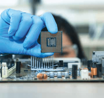
Aselsan produces its own wafers.Guys does Aselsan produce their own GaN wafers or do they import them ?

Latest Thread
- Germany German arms export licences for Israel surge with focus on sub project
- France Wildfire news and updates
- Casual Discussion Did You Know?
- Bangladesh Bangladesh building first research vessel to explore the Bay
- Bangladesh Bangladesh to build 108-km fence along Myanmar border
You are using an out of date browser. It may not display this or other websites correctly.
You should upgrade or use an alternative browser.
You should upgrade or use an alternative browser.
")

Metu is the only producer till now for fpa in turkey ..they produce IR fpa with qwip tech and gave the licence to aselsan .. its already in mass production since 2014 .. also they produce non cooled sensors with vox and arsenide tech .. these are the already serially produced fpa .. aselsan produced the prototype of cooled mct tech and it supposed to be serially produced in short time (on board tests were started last year) ... Also studies continue for mor advanced super lattice detectors for tfx programAnyone got a good source for IR FPA semiconductors ?
from left to right :kalkan II,erken ihbar radarı,alçak irtifa radarı,siper arama radarı,siper FCR,C-RAM radarı,portatif aesa,S,?-radarı,? uyarı radarı,? View attachment 34759
AURA AESA radar
Combat-Master
Baklava Consumer

Development of Uncooled Microbolometer Infrared Detector with 12 μm pixel pitch – (SSB project)
Within the scope of the project, a microbolometer Detector in 640 x 480 format with 12-micron pixel technology will be developed. The developed sensors will be vacuum-packed within the scope of service procurement at Aselsan and It will be tested with imaging hardware supplied from Mikro-Tasarim company. The project started in 2019, with funds being made available in early 2020.


Within the scope of the project, a microbolometer Detector in 640 x 480 format with 12-micron pixel technology will be developed. The developed sensors will be vacuum-packed within the scope of service procurement at Aselsan and It will be tested with imaging hardware supplied from Mikro-Tasarim company. The project started in 2019, with funds being made available in early 2020.
Last edited:
Excellent pixel width, but what is the bandwith ? Also I wonder how Aselsan make these detectors. TSMC ?Development of Uncooled Microbolometer Infrared Detector with 12 μm pixel pitch – (SSB project)
Within the scope of the project, a microbolometer Detector in 640 x 480 format with 12-micron pixel technology will be developed. The developed sensors will be vacuum-packed within the scope of service procurement at Aselsan and It will be tested with imaging hardware supplied from Mikro-Design company. The project started in 2019, with funds being made available in early 2020.
View attachment 34772 View attachment 34773
Combat-Master
Baklava Consumer
Some of the ongoing projects;

Uncooled Microbolometer - MT10212BD - 1024x768 12 μm pixel pitch -

Uncooled Microbolometer - MT10212BD - 1024x768 12 μm pixel pitch -
Last edited:
I see a big potential for medium size USVs.
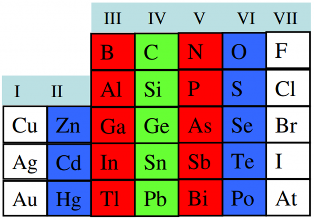
Semiconductors and Studies in Our Country #1 (2021)
What is Semiconductor?
Semiconductors; They are materials that are insulators under normal conditions, but whose conductivity properties can change (conductive) under certain conditions. The conductivity of semiconductors is affected by conditions such as temperature, electrical voltage, magnetic field, and light.
Some Semiconductor Elements and Compounds
Some of the semiconductors are compounds and some are elements.
Ge (Germanium), Si (Silicon),
GaAs (Gallium arsenide), GaP (Gallium phosphide), AlAs (Aluminum arsenide), InSb (Indium antimonite), InP (Indium phosphide), InAs (Indium arsenide), HgTe (Mercury (II) telluride), CdTe (Cadmium telluride) , CuO (Copper (II) oxide), SiC (Silicon carbide), GaN (Gallium nitride), CdS (Cadmium sulfide), PbS (Lead sulfide), SiGe (Silicon germanium), InGaAs (Indium gallium arsenide), HgCdTe (Mercury) cadmium telluride), ZnS (Tin sulfide), GaAlAs (Gallium aluminum arsenide), InAlAs (Indium aluminum arsenide), SiGeC (Silicon germanium carbide)…..
Organizations Working on Semiconductors in Our Country
YITAL
Within the framework of the heavy industry move started in the late 1970s, the necessity of an Integrated Circuit (IC) production factory was seen in our country and for this purpose, it was decided to establish a Semiconductor Circuit Element Factory (YIDEF) within the company TESTAŞ in Ankara. Initially, 7 µm (micrometer) Bipolar technology was transferred from a company in the USA and personnel were sent abroad for training. In parallel with these studies, YİTAL was established in 1983 within the Marmara Research Center (the Institute at that time) in the Gebze Campus of TÜBİTAK in order to solve possible problems in production and to develop new technologies.
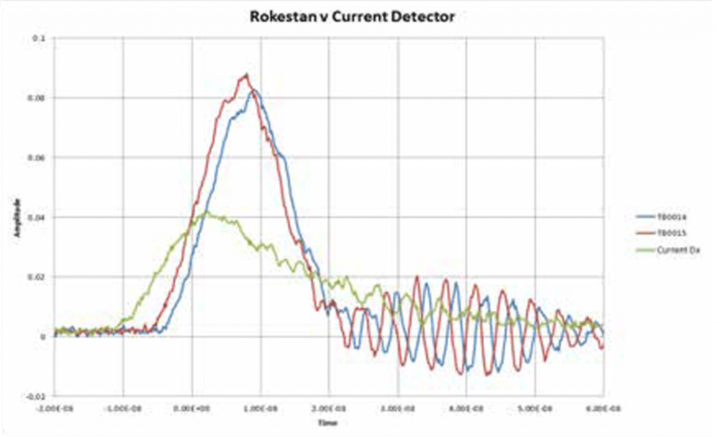
Our national semiconductor photodetectors have lower noise and higher reactivity than their counterparts produced abroad. In the production of semiconductor detectors, advanced semiconductor technology with 55 steps is used. Different types of detectors produced at BİLGEM are widely used by ROKETSAN, TÜBİTAK SAGE and ASELSAN. In line with the needs of our local industry, our detectors began to be sold abroad in 2019. The latest photodetector developed at BİLGEM has been successfully used in the Laser Approach Sensor of the HİSAR Missile.
YİTAL started the 0.25 µm SiGeC BiCMOS Cell Library Development Project in 2014 with the support of the SSB R&D Department. In 2018, the SiGe HBT process, in line with the project objectives (Ft: 125GHz and BVCE0: 1.7V), was successfully developed and its repeatability was proven. In 2019, a 0.25 µm CMOS process suitable for this process was developed. Subsequently, these two production lines were combined, and SiGe BiCMOS technology and RFIC ICs started to be implemented within the country.
YITAL has the infrastructure and a powerful device park that can apply 0.25 µm SiGe BiCMOS technology. These devices are installed in the clean-area consisting of 10, 100 and 1000 class zones with an area of 1000 m². Processes carried out in the clean area; mask production, wafer processing, flake yield map, integrated circuit sheathing and functional and burn-in tests. Used in semiconductor technology (chemical cleaning, high temperature oxidation, low pressure gas phase film deposition (LPCVD), plasma assisted film deposition (PECVD), physical film deposition (PVD), ion seeding, lithography, plasma assisted etching (RIE, All techniques are applied (such as ICP, chemical mechanical leveling (CMP)).
Integrated Circuit Design at YİTAL
YITAL digital design team has carried out the designs of digital ICs produced in YITAL with a full special design technique. In the fully special design technique, all the schematic and lay-out design at the transistor and gate level are done manually from the lowest level to the smallest area, highest speed and lowest power consumption. In this way, it is ensured that the technology is used at the limits and the lowest cost is obtained by increasing the number of ICs per wafer. The disadvantage of the full custom design technique is the long design time. Therefore, it is necessary to use automatic design flow in ICs containing many transistors. The laying of the digital blocks of the smart card, which is the only integrated circuit produced abroad
The design was made with a fully automatic design method.
The hybrid design method is used in the design of the special purpose processor containing millions of transistors, which is being studied to be produced at YİTAL. In hybrid design; While blocks with a modular repetitive structure and blocks in the timing-critical path are fully custom designed, non-modular structures such as control blocks are designed fully automatically. The designs of analog and RF circuits are also made exclusively at the transistor level.
YİTAL Design Department took part in the project called SCARD supported by the European Union (EU) 6th Framework Program and realized successful designs using a design technique resistant to side channel analysis. There are Smart Card ICs designed by YİTAL in our ID cards that are in use today.
Cleaning Processes in Integrated Circuit Production
Cleaning processes at YİTAL are mostly carried out before layer storage and thermal oxidation processes. The flake surface must be clean in order to carry out healthy storage and oxidation processes. It is important that the stamp is clean in terms of keeping the production tools clean. In addition, after some steps during production, cleaning processes are carried out to remove the reaction residues.
Piranha solution (Piranha Solution / SPM / Sulfuric Peroxide Mix) to remove organic waste on the silicon wafer; SC-1 (APM / Ammonia Peroxide Mixture) for cleaning of impurities and organic matter from the environment and equipment; SC-2 (HPM / Hydrochloric Peroxide Mixture) to remove various metal ions from semiconductor manufacturing processes by chemical reaction; dilute hydrofluoric acid (DHA / Dilute Hydrofluoric Acid) to corrode the natural oxide formed on the flake surface or chemically stored oxide; Components such as SPM, isopropyl alcohol and DHA are used for the chemical removal of by-products/polymers and photoresist (a light sensitive material) formed as a result of etching processes.
In addition to wet cleaning, dry cleaning is also carried out at YİTAL. Dry cleaning processes are carried out in plasma reactors. Oxygen gas is used to wipe the photoresist and remove the polymers formed after etching, and nitrogen fluoride gas is used to remove the natural oxide. After all these wet and dry cleaning processes, the flakes are washed and dried.
Integrated Circuit Production Ashers Process
Dry etching is carried out at YİTAL with 9 reactors with 3 different working principles. Typically, reactors are devices made of aluminium, glass or quartz, capable of descending into low vacuum. These devices basically include vacuum system consisting of reactor chamber, turbo pump and dry pump, radiofrequency (RF) power sources, water or gas cooling-heating systems and gas distribution systems. The flakes to be abraded are loaded into the reactor, the dry pump and turbopump vacuum the reactor, and the reactive gases are fed into the reactor. By ionizing the gases with radiofrequency (RF) energy, the conditions necessary for etching are created. The basic parameters of dry etching processes are temperature, pressure, power, gas flow rates and time. There are 3 RIE (Reactive Ion Etch / Reactive Ion Etching) reactors in YİTAL and these reactors are used in different stages of IC production.
YITAL has 2 ICP (Inductively Coupled Plasma / Inductively Coupled Plasma) reactors. In one of these reactors, polysilicon and metal layers (Aluminum, Titanium and Titanium nitrite) are eroded in the other. Hydrogen bromide, chlorine, oxygen and argon gases are used as corrosive gas. Hydrogen bromide and chlorine gas are the main corrosive gases for etching dissimilar metals and polysilicon. Oxygen accelerates the reaction or creates an anisotropic profile as specified in the RIE. Argon gas, on the other hand, contributes to the reaction rate and selectivity by etching it by physical bombardment.
Photolithography Process
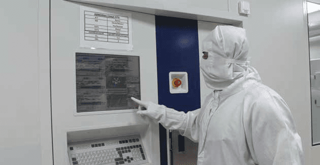
Photolithography is the process of transferring a pattern on a mask onto a mostly silicon wafer using an ultraviolet (UV), deep ultraviolet (DUV) or extreme ultraviolet (EUV) light source. The clean area where photolithography processes are carried out in YİTAL is in the class 10 category. At YİTAL, clean area temperature and humidity values are monitored with high precision and the necessary conditions for the photolithography process are provided.
GÜNAM
GÜNAM was established in 2009 with the initiative of Middle East Technical University (METU). DAY; It is the leading and most comprehensive national center with a mission to become a global player in the development of solar technologies. The technological know-how of GÜNAM, which does not transfer technology from outside, belongs to itself.
GÜNAM Photovoltaic Line
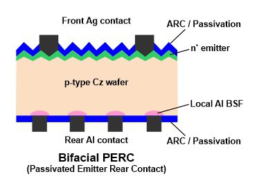
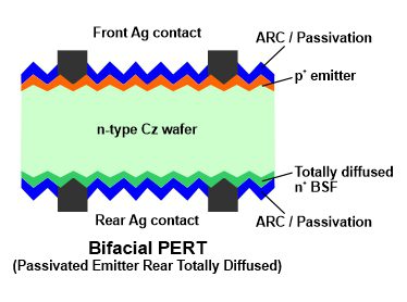
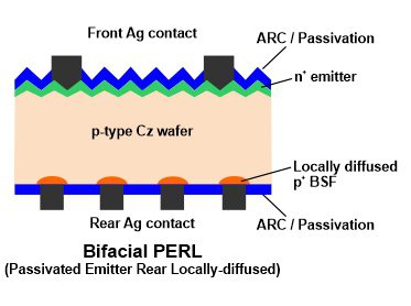
The new facility of GÜNAM (Solar Energy Research and Application Center) is GPVL (GÜNAM Photovoltaic Line / GÜNAM Photovoltaic Line); mainly c-Si (Crystalline Silicon / Crystal Silicon) such as PERC (Passivated Emitter and Rear Cell) / PERT (Passivated Emitter Rear Totally Diffused) / PERL (Passivated Emitter with Rear Locally Diffused) and IBC (Interdigitated Back Contact) type can produce solar panel cells (Solar Cell). GPVL; It serves as a pilot production line from the substrate (Wafer) to the solar panel cell. GPVL; It has an office area of 200 m² and a production area of 600 m².
Clean Room
The cleanroom in GÜNAM consists of four sections with a total laboratory area of 150 m². c-Si and Si (Silicon) based thin film (Thin Film) production tools are located in the main hall of the facility. There are separate rooms for Wet Chemical Processing and photolithography. There is also a room for testing and characterization. The clean room can produce industrial size crystalline silicon cells. It has several departments, including a photolithography facility for scientific research. Since 2012, all processes have been optimized by GÜNAM researchers to produce cells in this clean room.
Nanooptics Research Laboratory (NRL)
NRL's areas of work related to the production of fine crystalline silicon materials include:
Laser assisted slicing of crystalline silicon chips;
Crystallization of thin amorphous silicon layers with laser support;
Laser forming and processing of thin amorphous silicon layers
Crystal Silicon Cell Laboratory
Three-tube furnaces each, located in the Crystal Silicon-Based Cell Laboratory, are capable of processing twenty-five 6-inch round or square substrates at a time. In addition, this furnace contains a PECVD (Plasma-Enhanced Chemical Vapor Deposition) tube.
Thin Film Lab
Thin-film photovoltaic technologies have been developed to reduce material costs. There are several thin film technologies such as amorphous silicon or Cd/Te semiconductors. Research groups from different branches are working on thin film technologies at GÜNAM.
Characterization Laboratory
All cells are tested in the Optical and Electrical Characterization Laboratory during and after production. For optical characterization;
Reflection measurements (Diffuse and Specular);
Permeability measurements;
Photoconductivity measurements;
Film thickness measurements,
It can be made by researchers for wavelengths ranging from 100nm (nanometers) to 2μm.
In addition, there are 2 different solar simulators in GÜNAM laboratories.
GÜNAM's Silicon Cell Technology
PERC / PERT / PERL Cell
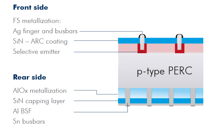
Single Faced PERC Cell
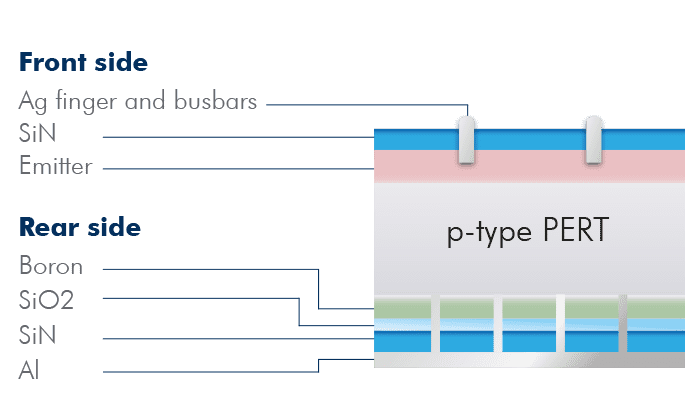
Single Faced PERT Cell
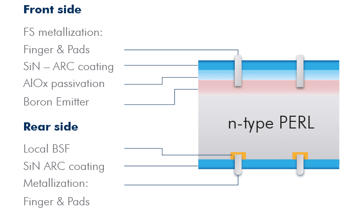
Single Faced PERL Cell
IBC Cell
Bifacial Cell
Two-Face PERC Cell
Two-Faced PERT Cell
Two-Face PERL Cell
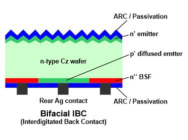
Two-Face IBC Cell
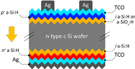
Silicon Heterojunction Cell
METU MEMS
Founded in 2008, METU MEMS (MicroElectroMechanical Systems) Research and Application Center; It has made it its mission to develop advanced technology solutions to provide scientific and economic added value to our country in the field of MicroElectroMechanical Systems.
METU MEMS Center
The technology defined as MicroElectroMechanical Systems, known as MEMS abbreviated, has the potential to change our age, just like microelectronics or microchip technology. Thanks to this technology, not only microelectronic integrated circuits but also micromechanical structures can be made on microchips. Thus, both microsensors and microactuators and electronic circuit can be made in a chip, and the system price and dimensions can be as cheap as a chip and as small as a chip. METU MEMS; works on components such as infrared sensors, gyrometer, accelerometer, magnetometer, RF switch, RF capacitor, adjustable circuit components, phase shifters, reshapeable antennas, antenna arrays.
Some Operations That Can Be Done at METU MEMS
Photolithography
Wet Etch
Plasma Ashers
Chemical Vapor Deposition with Plasma (PECVD)
Chemical Mechanical Etching (CMP)
PEROSOLAR
Founded in 2018, PeroSolar is a company that produces thin-film solar cells and researches and develops this technology. It is the only company that produces industrial perovskite solar cells in this field in Turkey. The company received a gold medal among 400 innovative projects in the EURO-INVENT 2019 Romania competition. PeroSolar can also manufacture thin-film flexible solar cells and panels. The company, which completed its solar cell R&D (Research and development) studies in 2019, is in the process of mass production. In addition, it continues to do R&D for the commercialization of this technology with its strong research and engineer team.
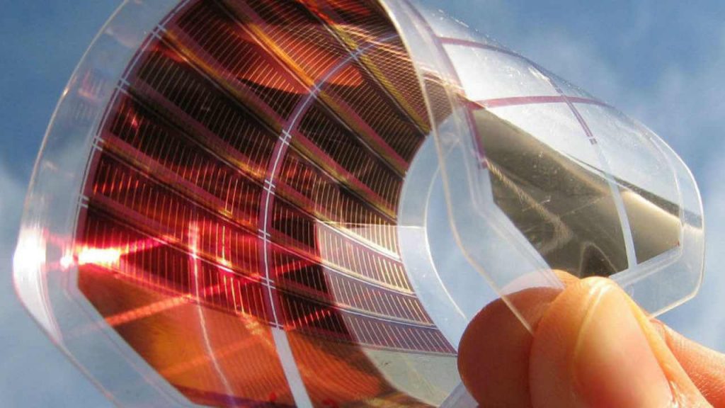
PeroSolar plans to open its pre-mass production facility with a perovskite cell production capacity of 1 MW/year in 2022. Their 2024 target is to open a facility with a perovskite cell production capacity of 300 MW/year. Cells that will be produced without the use of lead by PeroSolar will have an efficiency of 18-20%+. The 10x10cm perovskite cells developed by PeroSolar can produce 5 W (Watt) of energy. The solar panels to be produced are planned to have a power density of 250 W/m² and mass production at a cost of $ 0.05/W. The biggest advantage of perovskite cells is; They are flexible, can produce energy even when direct sunlight is not available, are more durable in space conditions (cosmic radiation), have low raw material costs and have low fabrication costs.
 teknotower.com
What is Semiconductor?
Semiconductors; They are materials that are insulators under normal conditions, but whose conductivity properties can change (conductive) under certain conditions. The conductivity of semiconductors is affected by conditions such as temperature, electrical voltage, magnetic field, and light.
Some Semiconductor Elements and Compounds
Some of the semiconductors are compounds and some are elements.
Ge (Germanium), Si (Silicon),
GaAs (Gallium arsenide), GaP (Gallium phosphide), AlAs (Aluminum arsenide), InSb (Indium antimonite), InP (Indium phosphide), InAs (Indium arsenide), HgTe (Mercury (II) telluride), CdTe (Cadmium telluride) , CuO (Copper (II) oxide), SiC (Silicon carbide), GaN (Gallium nitride), CdS (Cadmium sulfide), PbS (Lead sulfide), SiGe (Silicon germanium), InGaAs (Indium gallium arsenide), HgCdTe (Mercury) cadmium telluride), ZnS (Tin sulfide), GaAlAs (Gallium aluminum arsenide), InAlAs (Indium aluminum arsenide), SiGeC (Silicon germanium carbide)…..
Organizations Working on Semiconductors in Our Country
YITAL
Within the framework of the heavy industry move started in the late 1970s, the necessity of an Integrated Circuit (IC) production factory was seen in our country and for this purpose, it was decided to establish a Semiconductor Circuit Element Factory (YIDEF) within the company TESTAŞ in Ankara. Initially, 7 µm (micrometer) Bipolar technology was transferred from a company in the USA and personnel were sent abroad for training. In parallel with these studies, YİTAL was established in 1983 within the Marmara Research Center (the Institute at that time) in the Gebze Campus of TÜBİTAK in order to solve possible problems in production and to develop new technologies.
Our national semiconductor photodetectors have lower noise and higher reactivity than their counterparts produced abroad. In the production of semiconductor detectors, advanced semiconductor technology with 55 steps is used. Different types of detectors produced at BİLGEM are widely used by ROKETSAN, TÜBİTAK SAGE and ASELSAN. In line with the needs of our local industry, our detectors began to be sold abroad in 2019. The latest photodetector developed at BİLGEM has been successfully used in the Laser Approach Sensor of the HİSAR Missile.
YİTAL started the 0.25 µm SiGeC BiCMOS Cell Library Development Project in 2014 with the support of the SSB R&D Department. In 2018, the SiGe HBT process, in line with the project objectives (Ft: 125GHz and BVCE0: 1.7V), was successfully developed and its repeatability was proven. In 2019, a 0.25 µm CMOS process suitable for this process was developed. Subsequently, these two production lines were combined, and SiGe BiCMOS technology and RFIC ICs started to be implemented within the country.
YITAL has the infrastructure and a powerful device park that can apply 0.25 µm SiGe BiCMOS technology. These devices are installed in the clean-area consisting of 10, 100 and 1000 class zones with an area of 1000 m². Processes carried out in the clean area; mask production, wafer processing, flake yield map, integrated circuit sheathing and functional and burn-in tests. Used in semiconductor technology (chemical cleaning, high temperature oxidation, low pressure gas phase film deposition (LPCVD), plasma assisted film deposition (PECVD), physical film deposition (PVD), ion seeding, lithography, plasma assisted etching (RIE, All techniques are applied (such as ICP, chemical mechanical leveling (CMP)).
Integrated Circuit Design at YİTAL
YITAL digital design team has carried out the designs of digital ICs produced in YITAL with a full special design technique. In the fully special design technique, all the schematic and lay-out design at the transistor and gate level are done manually from the lowest level to the smallest area, highest speed and lowest power consumption. In this way, it is ensured that the technology is used at the limits and the lowest cost is obtained by increasing the number of ICs per wafer. The disadvantage of the full custom design technique is the long design time. Therefore, it is necessary to use automatic design flow in ICs containing many transistors. The laying of the digital blocks of the smart card, which is the only integrated circuit produced abroad
The design was made with a fully automatic design method.
The hybrid design method is used in the design of the special purpose processor containing millions of transistors, which is being studied to be produced at YİTAL. In hybrid design; While blocks with a modular repetitive structure and blocks in the timing-critical path are fully custom designed, non-modular structures such as control blocks are designed fully automatically. The designs of analog and RF circuits are also made exclusively at the transistor level.
YİTAL Design Department took part in the project called SCARD supported by the European Union (EU) 6th Framework Program and realized successful designs using a design technique resistant to side channel analysis. There are Smart Card ICs designed by YİTAL in our ID cards that are in use today.
Cleaning Processes in Integrated Circuit Production
Cleaning processes at YİTAL are mostly carried out before layer storage and thermal oxidation processes. The flake surface must be clean in order to carry out healthy storage and oxidation processes. It is important that the stamp is clean in terms of keeping the production tools clean. In addition, after some steps during production, cleaning processes are carried out to remove the reaction residues.
Piranha solution (Piranha Solution / SPM / Sulfuric Peroxide Mix) to remove organic waste on the silicon wafer; SC-1 (APM / Ammonia Peroxide Mixture) for cleaning of impurities and organic matter from the environment and equipment; SC-2 (HPM / Hydrochloric Peroxide Mixture) to remove various metal ions from semiconductor manufacturing processes by chemical reaction; dilute hydrofluoric acid (DHA / Dilute Hydrofluoric Acid) to corrode the natural oxide formed on the flake surface or chemically stored oxide; Components such as SPM, isopropyl alcohol and DHA are used for the chemical removal of by-products/polymers and photoresist (a light sensitive material) formed as a result of etching processes.
In addition to wet cleaning, dry cleaning is also carried out at YİTAL. Dry cleaning processes are carried out in plasma reactors. Oxygen gas is used to wipe the photoresist and remove the polymers formed after etching, and nitrogen fluoride gas is used to remove the natural oxide. After all these wet and dry cleaning processes, the flakes are washed and dried.
Integrated Circuit Production Ashers Process
Dry etching is carried out at YİTAL with 9 reactors with 3 different working principles. Typically, reactors are devices made of aluminium, glass or quartz, capable of descending into low vacuum. These devices basically include vacuum system consisting of reactor chamber, turbo pump and dry pump, radiofrequency (RF) power sources, water or gas cooling-heating systems and gas distribution systems. The flakes to be abraded are loaded into the reactor, the dry pump and turbopump vacuum the reactor, and the reactive gases are fed into the reactor. By ionizing the gases with radiofrequency (RF) energy, the conditions necessary for etching are created. The basic parameters of dry etching processes are temperature, pressure, power, gas flow rates and time. There are 3 RIE (Reactive Ion Etch / Reactive Ion Etching) reactors in YİTAL and these reactors are used in different stages of IC production.
YITAL has 2 ICP (Inductively Coupled Plasma / Inductively Coupled Plasma) reactors. In one of these reactors, polysilicon and metal layers (Aluminum, Titanium and Titanium nitrite) are eroded in the other. Hydrogen bromide, chlorine, oxygen and argon gases are used as corrosive gas. Hydrogen bromide and chlorine gas are the main corrosive gases for etching dissimilar metals and polysilicon. Oxygen accelerates the reaction or creates an anisotropic profile as specified in the RIE. Argon gas, on the other hand, contributes to the reaction rate and selectivity by etching it by physical bombardment.
Photolithography Process
Photolithography is the process of transferring a pattern on a mask onto a mostly silicon wafer using an ultraviolet (UV), deep ultraviolet (DUV) or extreme ultraviolet (EUV) light source. The clean area where photolithography processes are carried out in YİTAL is in the class 10 category. At YİTAL, clean area temperature and humidity values are monitored with high precision and the necessary conditions for the photolithography process are provided.
GÜNAM
GÜNAM was established in 2009 with the initiative of Middle East Technical University (METU). DAY; It is the leading and most comprehensive national center with a mission to become a global player in the development of solar technologies. The technological know-how of GÜNAM, which does not transfer technology from outside, belongs to itself.
GÜNAM Photovoltaic Line
The new facility of GÜNAM (Solar Energy Research and Application Center) is GPVL (GÜNAM Photovoltaic Line / GÜNAM Photovoltaic Line); mainly c-Si (Crystalline Silicon / Crystal Silicon) such as PERC (Passivated Emitter and Rear Cell) / PERT (Passivated Emitter Rear Totally Diffused) / PERL (Passivated Emitter with Rear Locally Diffused) and IBC (Interdigitated Back Contact) type can produce solar panel cells (Solar Cell). GPVL; It serves as a pilot production line from the substrate (Wafer) to the solar panel cell. GPVL; It has an office area of 200 m² and a production area of 600 m².
Clean Room
The cleanroom in GÜNAM consists of four sections with a total laboratory area of 150 m². c-Si and Si (Silicon) based thin film (Thin Film) production tools are located in the main hall of the facility. There are separate rooms for Wet Chemical Processing and photolithography. There is also a room for testing and characterization. The clean room can produce industrial size crystalline silicon cells. It has several departments, including a photolithography facility for scientific research. Since 2012, all processes have been optimized by GÜNAM researchers to produce cells in this clean room.
Nanooptics Research Laboratory (NRL)
NRL's areas of work related to the production of fine crystalline silicon materials include:
Laser assisted slicing of crystalline silicon chips;
Crystallization of thin amorphous silicon layers with laser support;
Laser forming and processing of thin amorphous silicon layers
Crystal Silicon Cell Laboratory
Three-tube furnaces each, located in the Crystal Silicon-Based Cell Laboratory, are capable of processing twenty-five 6-inch round or square substrates at a time. In addition, this furnace contains a PECVD (Plasma-Enhanced Chemical Vapor Deposition) tube.
Thin Film Lab
Thin-film photovoltaic technologies have been developed to reduce material costs. There are several thin film technologies such as amorphous silicon or Cd/Te semiconductors. Research groups from different branches are working on thin film technologies at GÜNAM.
Characterization Laboratory
All cells are tested in the Optical and Electrical Characterization Laboratory during and after production. For optical characterization;
Reflection measurements (Diffuse and Specular);
Permeability measurements;
Photoconductivity measurements;
Film thickness measurements,
It can be made by researchers for wavelengths ranging from 100nm (nanometers) to 2μm.
In addition, there are 2 different solar simulators in GÜNAM laboratories.
GÜNAM's Silicon Cell Technology
PERC / PERT / PERL Cell
Single Faced PERC Cell
Single Faced PERT Cell
Single Faced PERL Cell
IBC Cell
Bifacial Cell
Two-Face PERC Cell
Two-Faced PERT Cell
Two-Face PERL Cell
Two-Face IBC Cell
Silicon Heterojunction Cell
METU MEMS
Founded in 2008, METU MEMS (MicroElectroMechanical Systems) Research and Application Center; It has made it its mission to develop advanced technology solutions to provide scientific and economic added value to our country in the field of MicroElectroMechanical Systems.
METU MEMS Center
The technology defined as MicroElectroMechanical Systems, known as MEMS abbreviated, has the potential to change our age, just like microelectronics or microchip technology. Thanks to this technology, not only microelectronic integrated circuits but also micromechanical structures can be made on microchips. Thus, both microsensors and microactuators and electronic circuit can be made in a chip, and the system price and dimensions can be as cheap as a chip and as small as a chip. METU MEMS; works on components such as infrared sensors, gyrometer, accelerometer, magnetometer, RF switch, RF capacitor, adjustable circuit components, phase shifters, reshapeable antennas, antenna arrays.
Some Operations That Can Be Done at METU MEMS
Photolithography
Wet Etch
Plasma Ashers
Chemical Vapor Deposition with Plasma (PECVD)
Chemical Mechanical Etching (CMP)
PEROSOLAR
Founded in 2018, PeroSolar is a company that produces thin-film solar cells and researches and develops this technology. It is the only company that produces industrial perovskite solar cells in this field in Turkey. The company received a gold medal among 400 innovative projects in the EURO-INVENT 2019 Romania competition. PeroSolar can also manufacture thin-film flexible solar cells and panels. The company, which completed its solar cell R&D (Research and development) studies in 2019, is in the process of mass production. In addition, it continues to do R&D for the commercialization of this technology with its strong research and engineer team.
PeroSolar plans to open its pre-mass production facility with a perovskite cell production capacity of 1 MW/year in 2022. Their 2024 target is to open a facility with a perovskite cell production capacity of 300 MW/year. Cells that will be produced without the use of lead by PeroSolar will have an efficiency of 18-20%+. The 10x10cm perovskite cells developed by PeroSolar can produce 5 W (Watt) of energy. The solar panels to be produced are planned to have a power density of 250 W/m² and mass production at a cost of $ 0.05/W. The biggest advantage of perovskite cells is; They are flexible, can produce energy even when direct sunlight is not available, are more durable in space conditions (cosmic radiation), have low raw material costs and have low fabrication costs.
Yarıiletkenler ve Ülkemizdeki Çalışmalar #1 (2021) | TeknoTower
Yarıiletkenler; normal koşullar altında yalıtkan olan ancak belirli koşullar altında iletkenlik özellikleri değişebilen (iletken olan) materyallerdir.
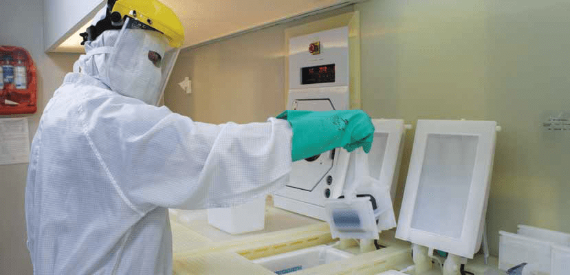
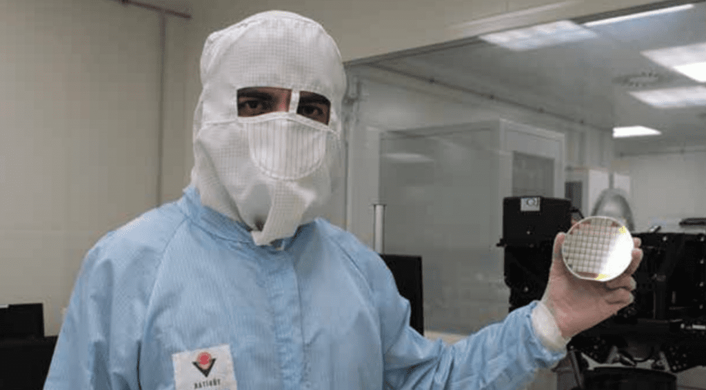
Aselsan has its own fab.Excellent pixel width, but what is the bandwith ? Also I wonder how Aselsan make these detectors. TSMC ?

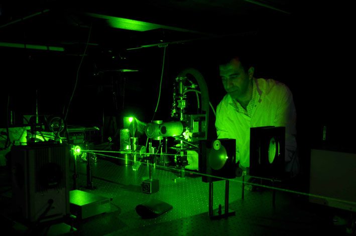
That lab shown is small like University labs (a small University lab!), not comparable with the chip production facilities of Korea and Malaysia. They can only produce limited amounts there and not even in nanometer scales
Combat-Master
Baklava Consumer
EWPOD F-16 - Jammer pod

Where did this project reach till now ?EWPOD F-16 - Jammer pod
View attachment 34815
M
Manomed
Guest
300 IQ move tbh lets not put the aesa on F16 özgürs lets put it on the Akıncı
AKINCI TİHA Integration of National AESA Radar Started


Combat-Master
Baklava Consumer
DDA-1 & DDA-2 - Semi Active Laser Seeker Detector


ARMOL TUMOL YGLS directed energy weapon systems

Electronic Warfare Tech

YITAL TUTEL

ARMOL TUMOL YGLS directed energy weapon systems
Electronic Warfare Tech
YITAL TUTEL
"All our forces decided to use CATS"
