
It's not that I disagree with the professor @Bogeyman quoted. China has been sanctioned heavily and has to develop the entire supply-chain itself. This is a humongous undertaking and the most important element is the lithography machines, imho. I wish their research would be more fruitful and we see a fully vertically-integrated chip manufacturing that will drive the price-gouging NVIDIA out of market. NVIDIA's cupidity has to end and the Chinese are the only hope so that I, maybe, can run my sidekick AI on my GPU clusters at home someday.
Chinese-made 7nm chips in Huawei phone raise questions over US export ban
The discovery of 7nm, 5G-enabled chips in Huawei’s latest phone has sparked an investigation by the US Commerce Department into how the country was able to acquire the technology.www.computerworld.com
Keep in mind this is still made with DUV machines, with a sort of tinkering to reach the limits of what duvs can offer. It's not as efficient as EUV 7nm chips (and the transistor size as the video mentions is most times a marketing gimmick as what Nvidia calls 10nm, intel can call 14nm and what they call 7nm, Nividia calls 5nm as the criteria they use for measurements are different; another crucial point is that transistor size is the most important factor for performance and efficiency of chips but it's not the only factor; manufacturing know-how in limiting power leakage, enhancing switching speeds, interconnect resistance and capacitance all matter. For power consumption there are also techniques independent of transistor size, like DVFS and some other technical stuff that I read about but I forgot. All in all this Huawei chip was not expected by West but it doesn't mean China has closed the gap by that much. They are still about 10 years behind (as the performance and techniques and machines used are more than a decade out of date; but still it shows unexpected speed of development).

Latest Thread
- USA The Defense Autonomous Warfare Group (DAWG) concept
- Defence Q&A Trying to ID this thermal battery
- Forum Announcement Security verification
- China Air-Force People's Liberation Army Air Force(China)
- China 82 deaths in Liushenyu Coal Mine gas explosion
You are using an out of date browser. It may not display this or other websites correctly.
You should upgrade or use an alternative browser.
You should upgrade or use an alternative browser.
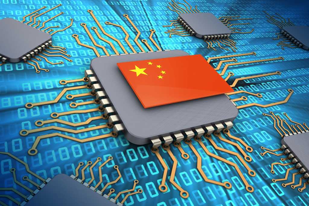
Microelectronics and Rare Earth Elements Sectors
- Thread starter Bogeyman
- Start date


It's not that I disagree with the professor @Bogeyman quoted. China has been sanctioned heavily and has to develop the entire supply-chain itself. This is a humongous undertaking and the most important element is the lithography machines, imho. I wish their research would be more fruitful and we see a fully vertically-integrated chip manufacturing that will drive the price-gouging NVIDIA out of market. NVIDIA's cupidity has to end and the Chinese are the only hope so that I, maybe, can run my sidekick AI on my GPU clusters at home someday.
Cost regarding that can only change if PRC manages to convince the world to adopt Yuan far more, so pricing can even attempt to bypass USD (and the vast seignoriage US has here by default).
Problem for PRC is its total debt level is already at 300% of GDP (this is huge problem showing up in real estate for a reason)....and thats all part of reason PRC holds onto US forex (just like Xi Jinping sending his daughter to harvard) against what it tries to broadcast instead.
Then there is problem of where the value addition is regarding these things. 10 billion out of 13 billion PRC earns from world in IP (with PRC still paying 45 billion to the world for their IP) was from huawei related comms. i.e there are huge tech tiers regarding the actual operationalising of the chips into products...compared to the component apex themselves. These are the things (human intellectual services related to the components) that are far more sanction proof in end too as they can be applied/licensed to other components (and their price levels defended in other countries etc).
PRC is lagging here, the paper publ. to IP earning ratio shows it....among the larger domestic fiscal problems PRC has grown for itself with its overwrought approach to statist control and bureaucracy.


US proposes restrictions for investments in Chinese tech, AI
The United States Department of the Treasury has fleshed out a proposed rule that would restrict and monitor US investments in China for artificial intelligence, computer chips and quantum computing.
The fleshed-out draft rule, issued on Friday, stems from President Joe Biden’s August executive order regarding the access that “countries of concern” have to American dollars to fund advanced technologies that could enhance those nations’ military, intelligence, surveillance and cyber-capabilities. The order identified China, Hong Kong and Macau as countries of concern.
The Biden administration has sought to stymie the development of technologies by China, the world’s second largest economy, that could give it a military edge or enable it to dominate emerging sectors such as electric vehicles (EVs).
In addition to the proposed rule, Biden, a Democrat, has also placed a stiff tariff on Chinese EVs, an issue with political implications as Biden and his Republican presidential opponent Donald Trump are both trying to show voters who can best stand up to China, a geopolitical rival and major trading partner.
The proposed rule outlines the required information that US citizens and permanent residents must provide when engaging in transactions in this area as well as what would be considered a violation of the restrictions.
It specifically would prohibit American investors from funding AI systems in China that could be used for weapons targeting, combat and location tracking, among other military applications, according to a senior Treasury official who previewed the rule for reporters on the condition of anonymity.
The US Treasury is seeking comment on the proposal through August 4 and after that is expected to issue a final rule.
Biden administration officials, including Treasury Secretary Janet Yellen, have insisted they have no interest in “decoupling” from China – however, tensions between the two nations have increased in recent years.
After the US military in February 2023 shot down a suspected Chinese spy balloon off the US East Coast after it traversed sensitive military sites across North America, China threatened repercussions.
Since then, incidents between the two nations based on national security concerns have regularly occurred.
For instance, Biden in May issued an order blocking a Chinese-backed cryptocurrency mining firm from owning land near a Wyoming nuclear missile base, calling its proximity to the base a “national security risk”.

US proposes restrictions for investments in Chinese tech, AI
Draft rule would bar US investment in AI systems in China that could be used for weapons targeting, other military uses.
China: World’s 1st light-based AI chip beats NVIDIA H100 in energy efficiency
Ateam of scientists from Beijing has announced a groundbreaking advancement in artificial intelligence (AI) technology with the development of the world’s first fully optical AI chip.This innovative chip, known as Taichi-II, represents a significant leap forward in both efficiency and performance, surpassing even the renowned NVIDIA Corp. NVDA H100 GPU in energy efficiency.
The research team, led by professors Fang Lu and Dai Qionghai from Tsinghua University, unveiled their findings on Wednesday.
A leap beyond: The Taichi-II chip’s superiority
The Taichi-II chip represents a substantial advancement from its predecessor, the Taichi chip, which had already set impressive records. Earlier this year, the researchers announced that the original Taichi chip had exceeded the energy efficiency of NVIDIA’s H100 GPU by over a thousand times, as reported by South Morning China Post (SCMP).Now, the Taichi-II chip has further elevated this benchmark, showcasing superior performance across various scenarios.
The study led by Professors Fang Lu and Dai Qionghai highlights Taichi-II’s capability to transform AI training and modeling. Unlike traditional methods that rely on electronic computers for training, the Taichi-II leverages optical processes, making it more efficient and significantly enhancing performance.
In practical terms, the Taichi-II chip has demonstrated remarkable advancements in several areas. It has expedited the training of optical networks containing millions of parameters by an order of magnitude and improved the accuracy of classification tasks by 40 percent.
In complex imaging scenarios, its energy efficiency in low-light conditions has improved by six orders of magnitude.
Innovative approach: FFM learning
The development of the Taichi-II chip is marked by its use of a novel approach called fully forward mode (FFM) learning. This technique allows for a computer-intensive training process to be conducted directly on the optical chip, enabling parallel processing of machine learning tasks.Xue Zhiwei, lead author of the study and a doctoral student, emphasized that this architecture supports high-precision training and is well-suited for large-scale network training.
“Our research envisions a future where these chips form the foundation of optical computing power for AI model construction,” Fang Lu stated.
The FFM learning method capitalizes on high-speed optical modulators and detectors, which could potentially outperform GPUs in accelerated learning scenarios. This innovation opens new possibilities for optical computing, moving it from theoretical concepts to practical, large-scale applications.
Implications and future prospects
The timing of Taichi-II’s debut is particularly notable. As the US has imposed restrictions on China’s access to advanced GPUs for AI training, the Taichi-II chip offers a viable alternative that could help mitigate these limitations.Additionally, the performance of Taichi-II comes amid reports that NVIDIA’s high-tech AI chips may be making their way into the hands of Chinese military officials, potentially influencing China’s technological advancements.

China develops 'world’s 1st' AI chip system powered entirely by light
Taichi-II demonstrates up to a thousandfold improvement in energy efficiency and accelerates AI training with cutting-edge optical processes.
Fully forward mode training for optical neural networks

Fully forward mode training for optical neural networks - Nature
We present fully forward mode learning, which conducts machine learning operations on site, leading to faster learning and promoting advancement in numerous fields.
 www.nature.com
World’s fastest memory writes 25 billion bits per sec, 10,000× faster than current tech
Aresearch team at Fudan University has built the fastest semiconductor storage device ever reported, a non‑volatile flash memory dubbed “PoX” that programs a single bit in 400 picoseconds (0.0000000004 s) — roughly 25 billion operations per second. The result, published today in Nature, pushes non‑volatile memory to a speed domain previously reserved for the quickest volatile memories and sets a benchmark for data‑hungry AI hardware.
Smashing the speed ceiling
Conventional static and dynamic RAM (SRAM, DRAM) write data in 1–10 nanoseconds but lose everything when power is cut. Flash chips, by contrast, hold data without power yet typically need micro‑ to milliseconds per write — far too slow for modern AI accelerators that shunt terabytes of parameters in real time.The Fudan group, led by Prof. Zhou Peng at the State Key Laboratory of Integrated Chips and Systems, re‑engineered flash physics by replacing silicon channels with two‑dimensional Dirac graphene and exploiting its ballistic charge transport.
By tuning the “Gaussian length” of the channel, the team achieved two‑dimensional super‑injection, which is an effectively limitless charge surge into the storage layer that bypasses the classical injection bottleneck.
“Using AI‑driven process optimization, we drove non‑volatile memory to its theoretical limit,” Zhou told Xinhua, adding that the feat “paves the way for future high‑speed flash memory.”
One billion cycles in a blink
Co‑author Liu Chunsen likens the breakthrough to shifting from a U‑disk that writes 1,000 times per second to a chip that fires 1 billion times in the blink of an eye. The previous world record for non‑volatile flash programming speed was about two million operations per second.Because PoX is non‑volatile, it retains data with no standby power, a critical property for next‑generation edge AI and battery‑constrained systems. Combining ultra‑low energy with picosecond write speeds could remove the long‑standing memory bottleneck in AI inference and training hardware, where data shuttling, not arithmetic, now dominates power budgets.
Industrial and strategic implications
Flash memory remains a cornerstone of global semiconductor strategy thanks to its cost and scalability. Fudan’s advance, reviewers say, offers a “completely original mechanism” that may disrupt that landscape.If mass‑produced, PoX‑style memory could eliminate separate high‑speed SRAM caches in AI chips, slashing area and energy. It can enable instant‑on, low‑power laptops and phones, and support database engines that hold entire working sets in persistent RAM.
The device can also strengthen China’s domestic drive to secure leadership in foundational chip technologies. The team did not disclose endurance figures or fabrication yield, but the graphene channel suggests compatibility with existing 2D‑material processes that global fabs are already exploring. “Our breakthrough can reshape storage technology, drive industrial upgrades and open new application scenarios,” Zhou said.
What happens next
Fudan engineers are now scaling the cell architecture and pursuing array‑level demonstrations. Commercial partners have not been named, but Chinese foundries are racing to integrate 2D materials with mainstream CMOS lines.If successful, PoX could come in as a new class of ultra‑fast, ultra‑green memories that meet the swelling appetite of large‑language‑model accelerators, finally giving AI hardware a storage medium that keeps pace with its logic.

China scientists develop flash memory 10,000× faster than current tech
PoX is a new class of ultra‑fast, ultra‑green memories that meet the swelling appetite of large‑language‑model accelerators.
Prof. Zhou Peng Fudan University
Subnanosecond flash memory enabled by 2D-enhanced hot-carrier injection
Abstract
The pursuit of non-volatile memory with program speeds below one nanosecond, beyond the capabilities of non-volatile flash and high-speed volatile static random-access memory, remains a longstanding challenge in the field of memory technology1. Utilizing fundamental physics innovation enabled by advanced materials, series of emerging memories2,3,4,5 are being developed to overcome the speed bottleneck of non-volatile memory. As the most extensively applied non-volatile memory, the speed of flash is limited by the low efficiency of the electric-field-assisted program, with reported speeds6,7,8,9,10 much slower than sub-one nanosecond. Here we report a two-dimensional Dirac graphene-channel flash memory based on a two-dimensional-enhanced hot-carrier-injection mechanism, supporting both electron and hole injection. The Dirac channel flash shows a program speed of 400 picoseconds, non-volatile storage and robust endurance over 5.5 × 10⁶ cycles. Our results confirm that the thin-body channel can optimize the horizontal electric-field (Ey) distribution, and the improved Ey-assisted program efficiency increases the injection current to 60.4 pA μm−1 at |VDS| = 3.7 V. We also find that the two-dimensional semiconductor tungsten diselenide has two-dimensional-enhanced hot-hole injection, but with different injection behaviour. This work demonstrates that the speed of non-volatile flash memory can exceed that of the fastest volatile static random-access memory with the same channel length.
Subnanosecond flash memory enabled by 2D-enhanced hot-carrier injection - Nature
A two-dimensional Dirac graphene-channel flash memory based on a two-dimensional-enhanced hot-carrier-injection mechanism that supports both electron and hole injection is used to make devices with a subnanosecond program speed.
www.nature.com
In-memory ferroelectric differentiator
Abstract
Differential calculus is the cornerstone of many disciplines, spanning the breadth of modern mathematics, physics, computer science, and engineering. Its applications are fundamental to theoretical progress and practical solutions. However, the current state of digital differential technology often requires complex implementations, which struggle to meet the extensive demands of the ubiquitous edge computing in the intelligence age. To face these challenges, we propose an in-memory differential computation that capitalizes on the dynamic behavior of ferroelectric domain reversal to efficiently extract information differences. This strategy produces differential information directly within the memory itself, which considerably reduces the volume of data transmission and operational energy consumption. We successfully illustrate the effectiveness of this technique in a variety of tasks, including derivative function solving, the moving object extraction and image discrepancy identification, using an in-memory differentiator constructed with a crossbar array of 1600-unit ferroelectric polymer capacitors. Our research offers an efficient hardware analogue differential computing, which is crucial for accelerating mathematical processing and real-time visual feedback systems.
In-memory ferroelectric differentiator - Nature Communications
Here, authors develop an in-memory differentiator using a 40×40 array of ferroelectric capacitors. This device efficiently performs real-time differential computation and motion extraction, demonstrating low energy consumption and high operational frequency, with potential applications in edge...
www.nature.com
@Sanchez @TR_123456 @Nilgiri @Yasar_TR @Strong AI
No need to hype it until we see an affordable scalability and mass production capability but this is the dream of every PC enthusiast, RAM and SSD as a single component.
China's magnet curbs risk halting Indian car production - industry documents
- Beijing restricted export of rare earth magnets in April
- Magnets used in automobiles, home appliances, clean energy
- Auto lobby says production may halt by end-May, early-June
- Industry wants govt help to ease curbs, expedite supplies
China, which controls over 90% of global processing capacity for the magnets used for automobiles, clean energy and home appliances, enacted restrictions in April requiring companies to obtain import permits from Beijing.
Though a response to U.S. President Donald Trump's tariffs, the export curbs will impact automakers globally. And Indian companies say a disruption in the world's third-largest car market is imminent due to rapidly depleting stocks and the onerous process of obtaining new supplies.
In a meeting with commerce ministry officials last week, the Society of Indian Automobile Manufacturers (SIAM), an industry group, said inventories at auto part makers are expected to run out by the end of May, according to an unreleased document seen by Reuters.
SIAM was seeking the intervention of Prime Minister Narendra Modi's government to help access magnets held at Chinese ports since April 4.
"Starting end May or early June, auto industry production is expected to come to a grinding halt," SIAM said in the document, which was presented during a May 19 meeting attended by executives from Maruti Suzuki, Mahindra & Mahindra and Tata Motors.
While China has cleared exports from some magnet producers, including Volkswagen (VOWG.DE), opens new tab suppliers, three auto industry executives told Reuters they fear strained relations between Beijing and New Delhi could hurt India's chances of getting quick approvals.
The company officials asked not to be identified due to the sensitivity of the issue.
When asked about the magnet restrictions' impact in India, China's embassy in New Delhi said it was "actively facilitating and streamlining compliant trade" in accordance with legal and regulatory requirements.
"China's lawful imposition of export controls on these items aims to better safeguard national security and interests," it said in a statement.
Mahindra (MAHM.NS), opens new tab, Maruti (MRTI.NS), opens new tab, Tata (TAMO.NS), opens new tab, SIAM and India's commerce and external affairs ministries did not respond to requests for comment. Neither did the Auto Component Manufacturers Association of India (ACMA), which also attended the meeting.
PERMIT HEADACHES
While rare earth magnets are a crucial component in electric vehicle motors, they are also required for parts like power windows and audio speakers used in traditional cars.And though the measures imposed by Beijing are meant to focus on high-performance exports, shipments of low-end magnets are also being held up at ports due to confusion around implementing the restrictions.
China's exports of permanent magnets fell 51% year on year to 2,626 tons in April, the first month of data following the curbs, customs data shows.
India's auto sector imported 460 tons of rare earth magnets, mostly from China, in the fiscal year ended March 31 and expects to import 700 tons worth $30 million this year, according to industry estimates.
"Though the cost of imported rare earth magnets is miniscule in vehicles, risk is vehicles cannot be manufactured even if we are short of one component," SIAM and ACMA said in a separate document submitted to the Indian government.
Indian companies are worried by the complexity of an import process that requires approvals from Indian ministries and documents including so-called "end-use certificates" stating the magnets are not for military purposes, the SIAM document said.
Those documents must be verified by the Chinese embassy in New Delhi and sent to companies' Chinese suppliers whereafter Beijing issues a licence, it added.
India should endorse applications from importers "within hours", the SIAM document said, and push the Chinese embassy and commerce ministry to approve them "on an urgent basis".
@TR_123456 @NilgiriChina's magnet curbs risk halting Indian car production - industry documents
NEW DELHI, May 28 (Reuters) - Indian auto production could grind to a halt within days due to Chinese export restrictions on rare earth magnets, according to company executives and documents from industry groups, which want the government to lobby Beijing to relax the curbs.
- Beijing restricted export of rare earth magnets in April
- Magnets used in automobiles, home appliances, clean energy
- Auto lobby says production may halt by end-May, early-June
- Industry wants govt help to ease curbs, expedite supplies
China, which controls over 90% of global processing capacity for the magnets used for automobiles, clean energy and home appliances, enacted restrictions in April requiring companies to obtain import permits from Beijing.
Though a response to U.S. President Donald Trump's tariffs, the export curbs will impact automakers globally. And Indian companies say a disruption in the world's third-largest car market is imminent due to rapidly depleting stocks and the onerous process of obtaining new supplies.
In a meeting with commerce ministry officials last week, the Society of Indian Automobile Manufacturers (SIAM), an industry group, said inventories at auto part makers are expected to run out by the end of May, according to an unreleased document seen by Reuters.
SIAM was seeking the intervention of Prime Minister Narendra Modi's government to help access magnets held at Chinese ports since April 4.
"Starting end May or early June, auto industry production is expected to come to a grinding halt," SIAM said in the document, which was presented during a May 19 meeting attended by executives from Maruti Suzuki, Mahindra & Mahindra and Tata Motors.
While China has cleared exports from some magnet producers, including Volkswagen (VOWG.DE), opens new tab suppliers, three auto industry executives told Reuters they fear strained relations between Beijing and New Delhi could hurt India's chances of getting quick approvals.
The company officials asked not to be identified due to the sensitivity of the issue.
When asked about the magnet restrictions' impact in India, China's embassy in New Delhi said it was "actively facilitating and streamlining compliant trade" in accordance with legal and regulatory requirements.
"China's lawful imposition of export controls on these items aims to better safeguard national security and interests," it said in a statement.
Mahindra (MAHM.NS), opens new tab, Maruti (MRTI.NS), opens new tab, Tata (TAMO.NS), opens new tab, SIAM and India's commerce and external affairs ministries did not respond to requests for comment. Neither did the Auto Component Manufacturers Association of India (ACMA), which also attended the meeting.
PERMIT HEADACHES
While rare earth magnets are a crucial component in electric vehicle motors, they are also required for parts like power windows and audio speakers used in traditional cars.
And though the measures imposed by Beijing are meant to focus on high-performance exports, shipments of low-end magnets are also being held up at ports due to confusion around implementing the restrictions.
China's exports of permanent magnets fell 51% year on year to 2,626 tons in April, the first month of data following the curbs, customs data shows.
India's auto sector imported 460 tons of rare earth magnets, mostly from China, in the fiscal year ended March 31 and expects to import 700 tons worth $30 million this year, according to industry estimates.
"Though the cost of imported rare earth magnets is miniscule in vehicles, risk is vehicles cannot be manufactured even if we are short of one component," SIAM and ACMA said in a separate document submitted to the Indian government.
Indian companies are worried by the complexity of an import process that requires approvals from Indian ministries and documents including so-called "end-use certificates" stating the magnets are not for military purposes, the SIAM document said.
Those documents must be verified by the Chinese embassy in New Delhi and sent to companies' Chinese suppliers whereafter Beijing issues a licence, it added.
India should endorse applications from importers "within hours", the SIAM document said, and push the Chinese embassy and commerce ministry to approve them "on an urgent basis".

A China move risked leaving Indian car production dead in its tracks
India's car production faced risk due to China's export restrictions on rare earth magnets. These magnets are vital for car components. SIAM urged government intervention to ease restrictions. China controls most of the global processing capacity. India imports a significant amount of these...
However, ET had reported citing sources that imports of permanent magnets used in cars and other electronics from China have likely resumed after India began issuing certificates assuring compliance with China’s export curbs. Officials said the Directorate General of Foreign Trade (DGFT) has issued around 30 certificates, one for each consignment, confirming that these permanent magnets would not be used for defence applications nor re-exported to the United States.
While the curbs primarily target high-performance magnets, shipments of low-end magnets have also been held up amid confusion over how the new rules should be implemented.
Low end magnets can be invested and shifted away more easily than high-end magnets (for EVs, defense tech etc). So not a huge long term threat to non-EV automobile industry, the issue was transient one for low-end compared to high-end.
Though India has to work with other large partners to address the long term vulnerability and develop rare earth supply chains in other parts of world.
India, Australia, US have the Quad synergy to unlock going foward:

Rare Earths Reserves: Top 8 Countries
The outlook for rare earths is supported by strong supply and demand fundamentals as the world heads into a new economic era with a focus on clean energy and technological advancements.But with supply chain worries rising, it’s worth looking at which countries have the highest rare earths...
 investingnews.com
TSMC's Arizona factory has quietly failed—$40 billion burned through, yield rate less than half of Japan's plants
The mainstream narrative is "America's semiconductor reshoring has succeeded." But the real data tells the complete opposite story—TSMC's Arizona operations have invested $40 billion over 3 years, with Q1 2026 yield at just 52%, compared to 95% at Japan's Kumamoto plant and 98% in Taiwan's home base; the gap is so wide it can't even be called a factory.
Issue 1: Talent training is nowhere near complete. TSMC transferred 1,500 engineers from Taiwan for rotational support, but the 6,000 locally hired U.S. employees require an average training cycle of 4-6 years—American universities don't even have a "semiconductor production line engineer" major.
Issue 2: The supply chain hasn't kept up. High-purity photoresists, specialty gases, ultra-clean chemicals—80% sourced from Japan, 20% from Taiwan. The Arizona plant's comprehensive cost per wafer is 1.6 times that of the Tainan plant.
Issue 3: Customers are voting with their feet. Apple and AMD originally committed to shifting high-end orders to Arizona, but in Q2 2026, they only placed 15% of the planned orders—the rest are still all produced in Taiwan. "Political correctness" can't override the economic math.
What does TSMC say internally? Morris Chang warned as early as 2023: "Arizona is a waste." Current CEO C.C. Wei recently admitted for the first time that "the U.S. plant's progress is not as expected"—this is the most candid self-criticism from a TSMC executive in 30 years. Semiconductor reshoring isn't something America can just will into existence; it's the result of 50 years of industrial accumulation, not something $400 billion in subsidies can buy.

At least the Kumamoto plant is a success.
TSMC's Arizona factory has quietly failed—$40 billion burned through, yield rate less than half of Japan's plants
The mainstream narrative is "America's semiconductor reshoring has succeeded." But the real data tells the complete opposite story—TSMC's Arizona operations have invested $40 billion over 3 years, with Q1 2026 yield at just 52%, compared to 95% at Japan's Kumamoto plant and 98% in Taiwan's home base; the gap is so wide it can't even be called a factory.
Issue 1: Talent training is nowhere near complete. TSMC transferred 1,500 engineers from Taiwan for rotational support, but the 6,000 locally hired U.S. employees require an average training cycle of 4-6 years—American universities don't even have a "semiconductor production line engineer" major.
Issue 2: The supply chain hasn't kept up. High-purity photoresists, specialty gases, ultra-clean chemicals—80% sourced from Japan, 20% from Taiwan. The Arizona plant's comprehensive cost per wafer is 1.6 times that of the Tainan plant.
Issue 3: Customers are voting with their feet. Apple and AMD originally committed to shifting high-end orders to Arizona, but in Q2 2026, they only placed 15% of the planned orders—the rest are still all produced in Taiwan. "Political correctness" can't override the economic math.
What does TSMC say internally? Morris Chang warned as early as 2023: "Arizona is a waste." Current CEO C.C. Wei recently admitted for the first time that "the U.S. plant's progress is not as expected"—this is the most candid self-criticism from a TSMC executive in 30 years. Semiconductor reshoring isn't something America can just will into existence; it's the result of 50 years of industrial accumulation, not something $400 billion in subsidies can buy.
I used to talk with an engineer from the Kumamoto plant (Chinese, living in Japan and working for a US company). He said almost all of the team are former employees of TSMC.
Even in North America, more than 70% of the researchers in AI/chips are Asian, whether Chinese, Japanese, Korean, or Indian.
Americans are paying the price for their education system breakdown.